
This project investigates the analysis and design of individual RF modules that are utilized in an idealized quadrature demodulator. For a given frequency range of operation, appropriate networks are implemented to match loads, filter certain frequency bands, split power in the system, and create phase shifted copies of selected signals. The design procedure of each module is rationalized, and the accompanying schematics, simulated data, and microstrip schematics are presented. Non-idealities such as lumped component tolerance and microstrip parasitic effects are considered, and methods are developed to account for these effects such as Monte-Carlo analysis and parameter optimization using gradient descent.
Introduction
A quadrature demodulator system is implemented in microstrip using both lumped and distributed element networks.The system is composed of five different modules (see Figure 1. First, an ultra-wideband antenna receives RF signals in the frequency range of $5.7$ GHz to $6.2$ GHz, with a \(50\:\Omega\) input impedance over this bandwidth. Module A consists of a bandpass filter that filters incoming signals with a maximally flat response over the antenna bandwidth. The signal is then sent to a low-noise amplifier, which is subsequently carried via an in-phase power dividing network (Module B) to interface with frequency mixers of nominal impedance \(50\:\Omega\). Each mixer is fed by either a \(90 ^\circ\) or \(0 ^\circ\) copy of a signal from a \(5.95\) GHz local oscillator. Signals originating from the local oscillator (LO) are phase-shifted using a quadrature power dividing network (Module C). The LO has an output impedance of \(100 -\textrm{j}120\:\Omega\) which must be matched to the nominal system impedance of \(50\:\Omega\) using a matching network (Module D). Finally, the output of each mixer is fed to low-pass filters (Module E) requiring a cutoff frequency of \(0.25\) GHz and \(60\) dB of attenuation at \(0.65\) GHz.
For each of the modules (A-E), the choice of specific designs and processes are explained. Detailed schematics, tables, and microstrip implementations to scale are provided for each module, along with relevant component values and simulations validating the design. Module A includes a Monte Carlo analysis to study the effects lumped component tolerance has on the filter performance. Additionally, parasitic effects from microstrip junctions were found to effect the behavior of certain modules, causing them to not meet performance specifications. To overcome this, the optimization tool built into Keysight Advanced Design System was used to tweak component parameters until a satifactory design was realized. Lastly, microstrip components were designed on Rogers TC\(350+\) with a substrate thickness of \(0.762\) mm, ports interfacing to each module are assumed to be of a nominal \(50\:\Omega\) characteristic impedance, and lumped elements are available in \(0402\) (\(1.0\) x \(0.5\) mm) for microstrip implementations.
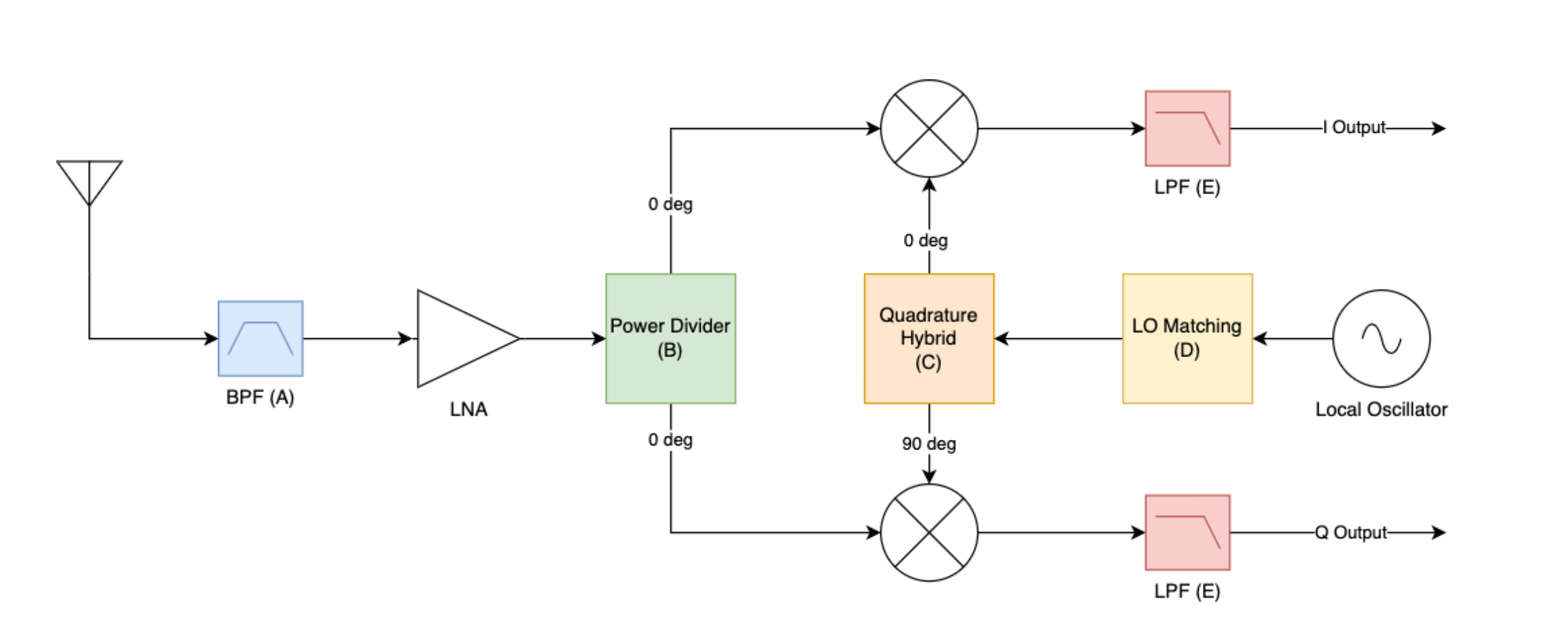 Figure 1 - System block diagram of an idealized quadrature demodulator.
Module A: Band-Pass Filter
A bandpass filter is required for the system characterized by a center frequency of \(f_0 = 5.95\) GHz and spanning the frequency range \(5.7\) GHz to \(6.2\) GHz. The design is specified to be of order \(N = 5\) with a maximally flat response.
Band-Pass Filter Design
The design of RF filters often involves making use of low-pass prototypes. The component values for each reactive element of an Nth order filter is selected in order to achieve a specific response behavior, such as steep roll-off in the stop-band or maximally flat ripple in the pass-band. Once the prototype is established, it is simply scaled in frequency and impedance to reach the desired performance parameters of the system. In this case, a maximally flat pass-band response is desired in a 5th order band-pass filter. A Butterworth prototype is first laid out, and then scaled in impedance and frequency to reach the desired band-pass characteristics. Figure 2 shows the low-pass prototype, with appropriate normalized component values for a 5th order Butterworth filter selected from 1 listed in the below table with values \(g1-g5\).
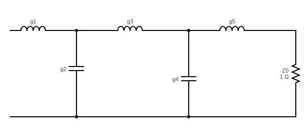 Figure 2 - Module A: Low-pass prototype beginning with series element.
| g1 | g2 | g3 | g4 | g5 |
|---|---|---|---|---|
| 0.6180 | 1.6180 | 2 | 1.6180 | 0.6180 |
The low-pass prototype is converted to a band-pass filter using component transformations given in 1. Series inductors are interchanged with series LC components, while shunt capacitors are interchanges with parallel LC components. This is seen in Figure 3, with the accompanying reactive component equations displayed.
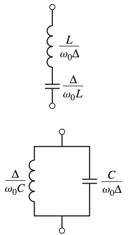 Figure 3 - Module A: (top) Band-pass transformation for series inductor. (bottom) Band-pass transformation for shunt capacitor
Applying these component-wise transformations to the elements of Figure (1) leads to following schematic for the band-pass filter design:
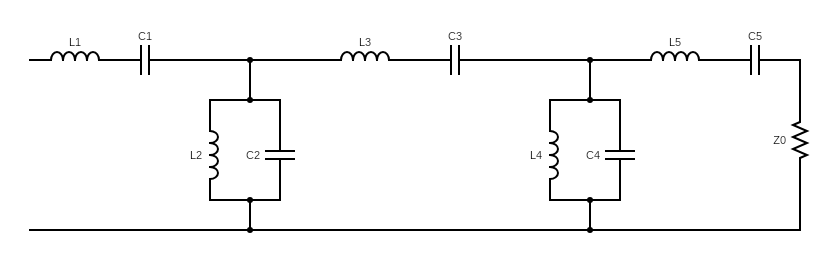 Figure 4 - Module A: 5th order Butterworth bandpass filter with center frequency of f = \(5.95\) GHz and spanning the frequency range \(5.7\) GHz to \(6.2\) GHz
The values of corresponding values for $L$ and $C$ are derived from the low-pass prototype values given in Table 1, and are summarized here in Table 2:
| L1, nH | C1, fF | L2, nH | C2, fF | L3, nH | C3, fF | L4, nH | C4, fF | L5, nH | C5, fF |
|---|---|---|---|---|---|---|---|---|---|
| 9.839 | 72.72 | 69.43 | 10.30 | 31.84 | 22.47 | 69.43 | 10.30 | 9.839 | 72.72 |
BPF Validation
The design of the band-pass filter is verified using simulation software in order to see how well the design performs with respect to the pass-band frequency range and ripple level. The circuit shown in Figure 4 and the accompanying components are implemented in ADS, and the transmission coefficient \(\textrm{S}_{21}\) is studied.
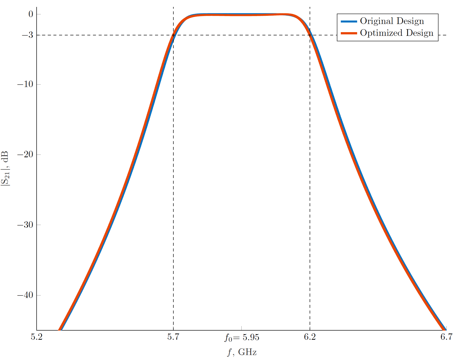 Figure 5 - Module A: \(|S_{21}|\), dB vs. frequency: Band-pass filter for module A.
From Figure 5, it is clear that the design performs extremely close to the design specifications. The original implementation was found to be around \(\pm1\) dB to high/low at the band-edges, so an optimization routine was run to get a value of \(-3\) dB at the cutoff, which is expected for Butterworth filters. Additionally, the filter remains less than \(-0.05\) dB in the pass-band, indicating nearly ideal transmission.
Lumped Component Tolerance: Monte Carlo Analysis
It is well-known that lumped elements posses a tolerance percentage indicating how much a given component will differ from its nominal design value. At high frequencies, this can significantly impact the performance of the system. To study this behavior, a Monte Carlo analysis is run for \(2000\) iterations on all of the lumped-elements involved in the band-pass filter simulation at three fixed frequencies of interest. Components of both \(2\%\) and \(5\%\) tolerance are considered in order to demonstrate the sensitivity band-pass filters have to component value perturbations.
The Butterworth band-pass filter is characterized by its center and edge-frequencies, so these regions are studied with respect to lumped component tolerances. First, the effect tolerance has on the value of \(S21\) at the band-edges are considered. Next, the effect tolerance has on the location of the center frequency \(f_0\) is studied.
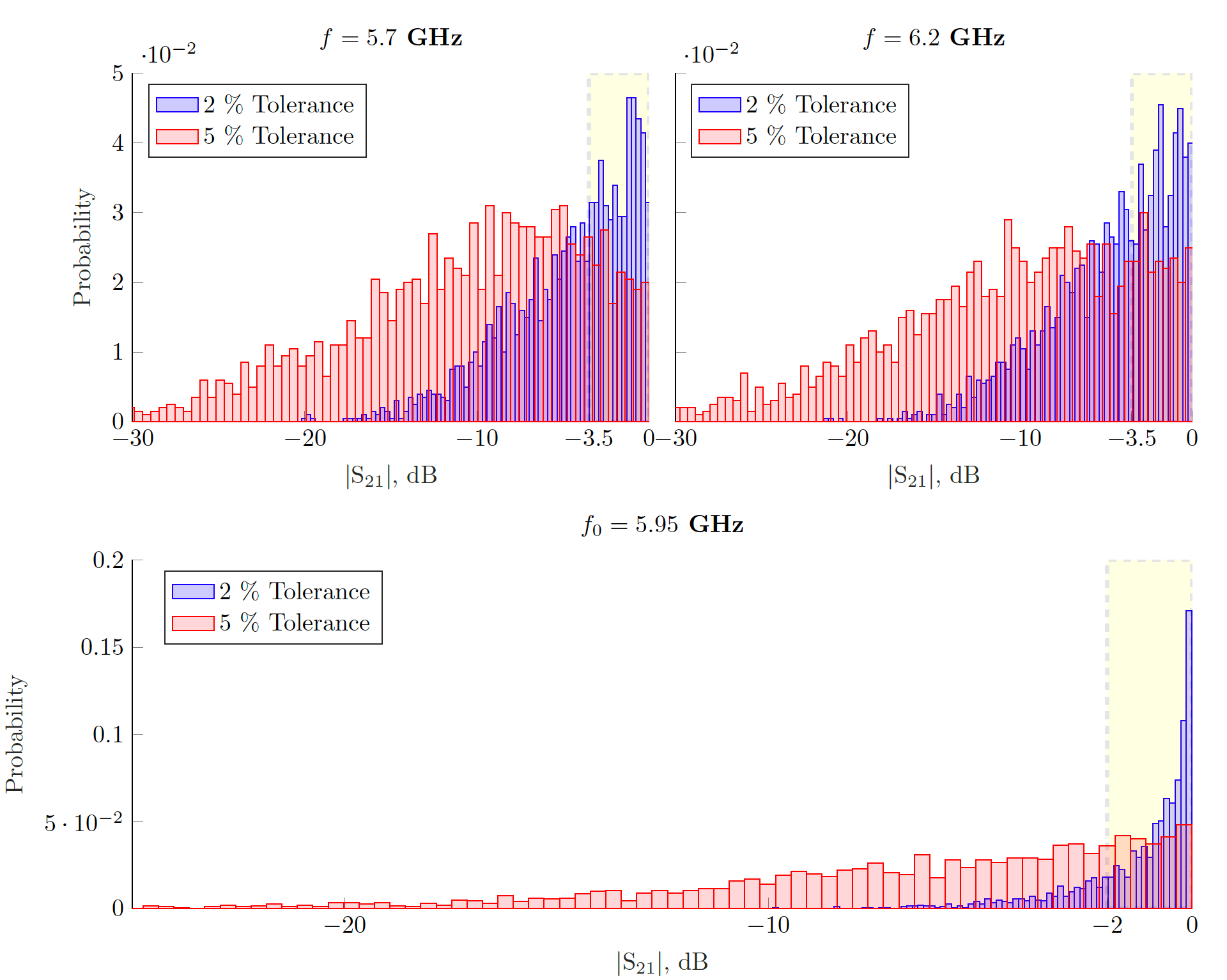 Figure 6 - Histograms specifying percentage of designs that achieve specific $|S21|$, dB ranges for low edge-frequency \(f = 5.7\) GHz (top left), high edge-frequency \(f = 6.2\) GHz (top right) and center frequency \(f= 5.95\) GHz (bottom).
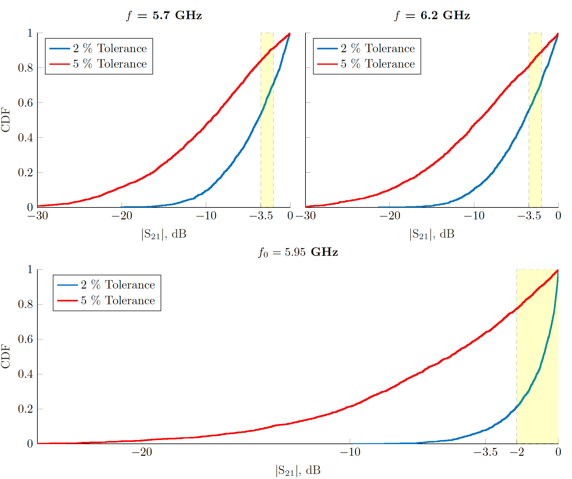 Figure 7 - Cumulative Density functions specifying percentage of designs that achieve specific \(|S21|\), dB ranges for low edge-frequency \(f = 5.7\) GHz (top left), high edge-frequency \(f = 6.2\) GHz (top right) and center frequency \(f= 5.95\) GHz (bottom).
From Figures 6 and 7 it is clear to see that even small tolerance variation in the lumped components can largely influence the filter performance. To quantify this, the percentage of designs meeting specific \(S21\) range criteria are looked at. For the edge frequencies, the percentage of designs that fall within \(-3.5\) and \(-2\) dB. For the left-edge frequency of \(f = 5.7\) GHz, it is observed that \(18\%\) of designs fall within \(-3.5\) and \(-2\) dB for \(2\%\) tolerance, and only \(7\%\) of designs fall within \(-3.5\) and \(-2\) dB for \(5\%\) tolerance. For the right-edge frequency of \(f = 6.2\) GHz, it is observed that \(17.7\%\) of designs fall within \(-3.5\) and \(-2\) dB for \(2\%\) tolerance, and only \(10\%\) of designs fall within \(-3.5\) and \(-2\) dB for \(5\%\) tolerance. For the center frequency of \(f_0 =5.95\) GHz, it is observed that \(79.41\%\) of designs fall within \(-2\) and \(0\) dB for \(2\%\) tolerance, and only \(24.2\%\) of designs fall within \(-2\) and \(0\) dB for \(5\%\) tolerance.
This Monte Carlo analysis reveals that the band-pass filter implemented with lumped-elements is highly influenced with component tolerances, and even small component tolerances can have a significant impact on the filter performance. As such, this design would suffer if it were to be mass-produced as the performance is somewhat unreliable when component tolerance is allowed. It may be more feasible to implement this module using a distributed element method in order to overcome the effect of lumped-component tolerance at the cost of physical dimension tolerances introduced by microstrip implementations.
Microstrip Implementation Figure
In a microstrip system, this band-pass filter would be realized using chip inductors and capacitors. A figure, approximately to scale, of this system is shown here in Figure 8.
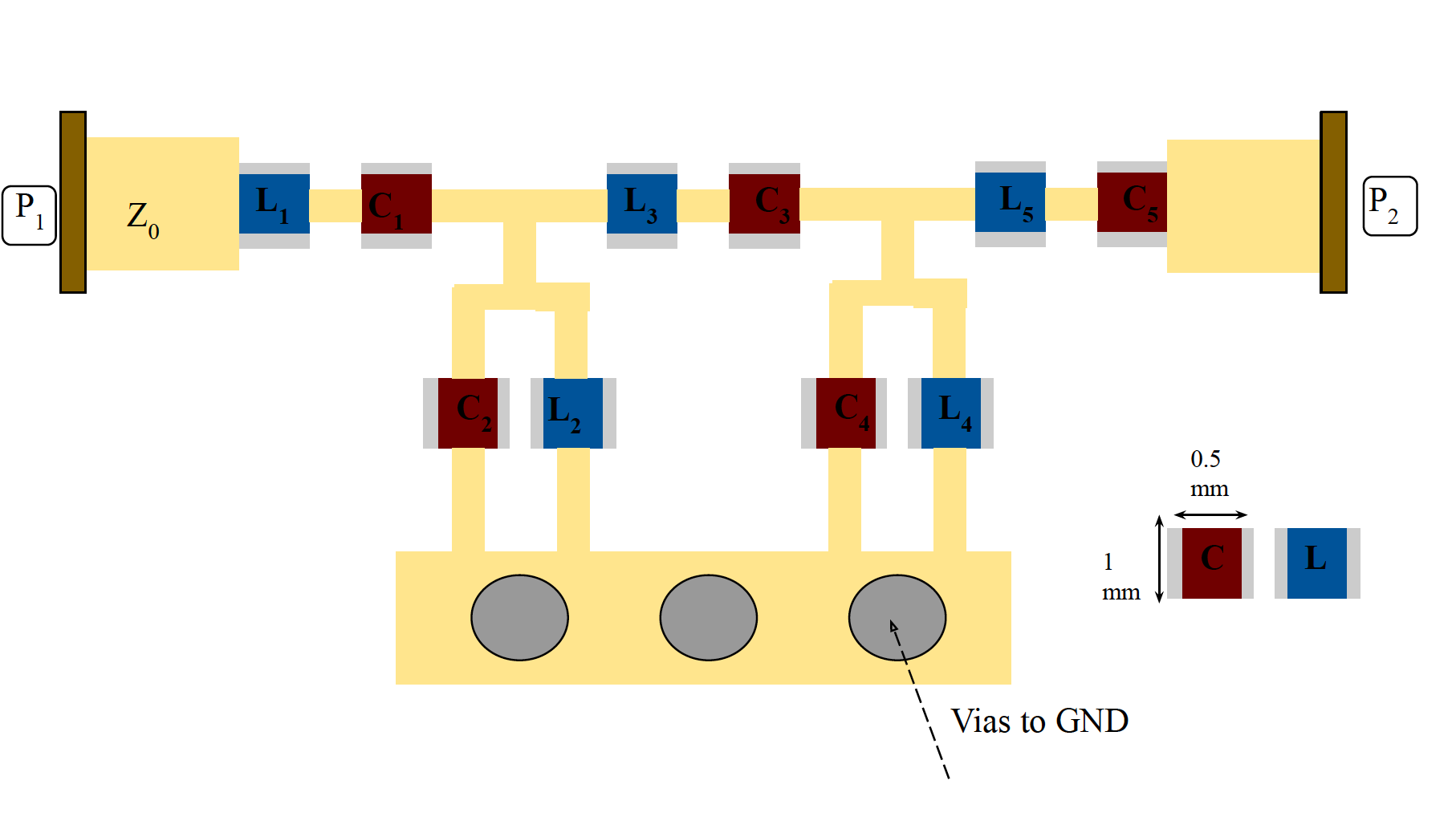 Figure 8 - Module A: Microstrip Implementation of the band-pass filter. (P1 = Port 1, P2 = Port 2)
Module B: In-Phase Power Dividing Network
The signal received and filtered by Module A must be split evenly and in phase using a power-divider network. This is realized here in Module B with the use of a T-Junction power divider. A T-Junction power divider is a lossless and reciprocal three port network that splits an input signal in-phase to two different output ports. This system was chosen over other in-phase splitters because of its simple topology that only relies on microstrip geometry and no additional lumped components.
T-Junction Design
A schematic for the lossless T-Junction power divider is given here in Figure 9.
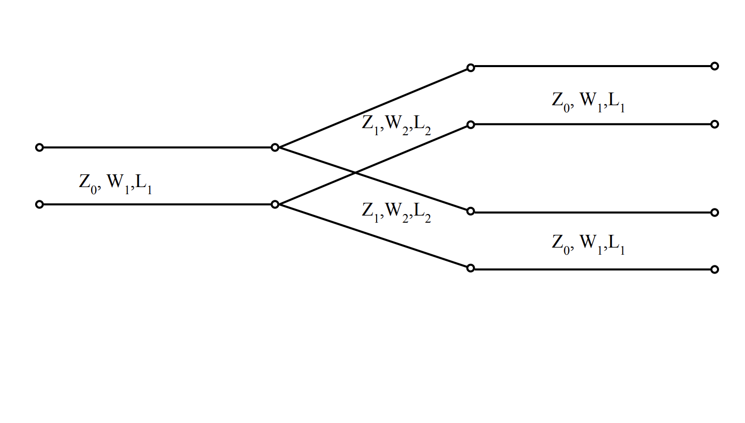 Figure 9 - Circuit schematic for a lossless T-Junction power divider.
Since this implementation is done in microstrip, the relevant widths and lengths of each line must be specified in order to design for specific characteristic impedance’s and electrical lengths. A T-Junction powder divider takes a power from a nominal input of \(Z_0\) and splits it to two output ports, in this case having nominal impedance $Z_0$. This system evenly splits the input signal to the output ports, which requires the input impedance looking into port 1 to be \(\textrm{Z}_{\textrm{in}} = 100\:\Omega\), which is the parallel combination of the output ports. This subsequently means that port 1 is matched if it has a nominal impedance of \(Z_0 = 50\:\Omega\). The S-Parameters of this system are given by the following:
\[\mathbf{S}=\frac{1}{2}\left[\begin{array}{lll} 0 & 1 & 1 \\ 1 & 0 & 1 \\ 1 & 1 & 0 \end{array}\right] \tag{1}\]The relevant system values for the T-Junction that realize these scattering parameters at the given design frequency and impedance’s are specified in Table 3:
| Design | \(\textrm{Z}_0, \: \Omega\) | \(\textrm{Z}_1= \textrm{Z}_0\sqrt{2}\:\Omega\) | \(\textrm{W}_1\), mm | \(\textrm{W}_2\), mm | \(\textrm{L}_1\), mm | \(\textrm{L}_2 = \lambda/4\), mm |
|---|---|---|---|---|---|---|
| Original | 50 | 70.71 | 1.725 | 0.940 | 7.534 | 7.719 |
| Optimized | 50 | 70.71 | 1.725 | 0.940 | 5.887 | 7.049 |
T-Junction Validation
The system given by the topology of Figure 9 with values from Table 3 were implemented in ADS in order to study the design performance. Additionally, MTEE, MBEND, and MSTEP elements were used in ADS in order to simulate the parasitic junction effects.
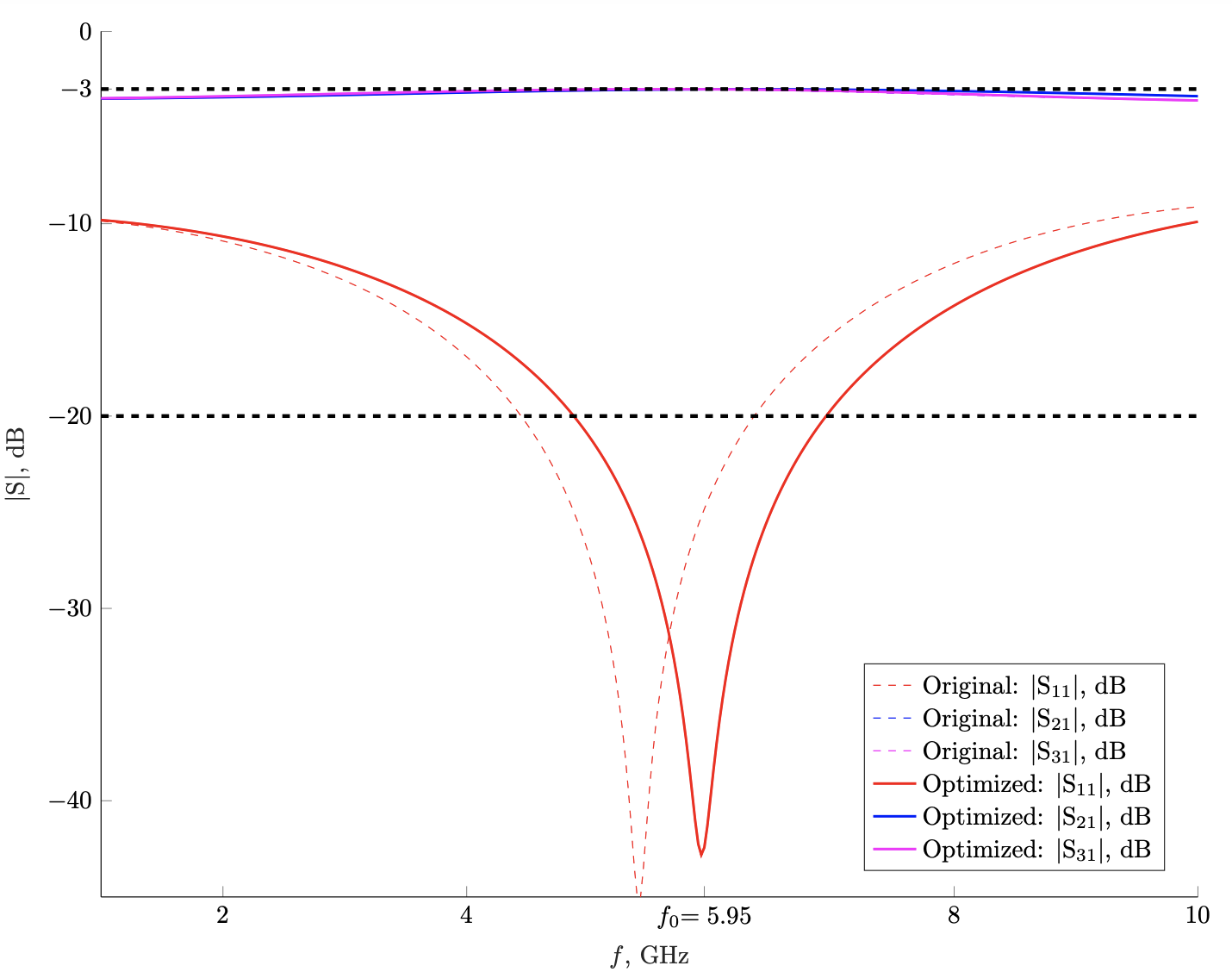 Figure 10 - Module B: S-Parameters for the T-Junction power divider for both the original and optimized designs.
The given design is refined using the optimizer in ADS in order to realize a performance close to the design specifications. From Figure 12, we can see that the original and optimized design have excellent half-power splitting performance over nearly all frequencies. Additionally, it is seen that the original design has the best port 1 match at a frequency slightly lower than the design specification. This is due parasitic effects arising at the junction of the power-divider, leading to additional resonance behavior which subsequently changes the match of the system. The optimizer was setup such that it was able to adjust the lengths of each microstrip segment until the desired performance is achieved, as seen in Table 3.
Note: Changing lengths will indeed change the phase difference between the transmitted signals to ports two and three. Since this system requires the outputs to be in phase, this is an important factor to consider. This change of phase was not accounted for in the optimization design, but it is understood that this change occurs. As such, only the phase of the original system design is studied here.
The phase difference of the outputs is also studied, as the input signal at port 1 of the T-Junction is designed such that the outputs at ports 2 and 3 are in phase with one another.
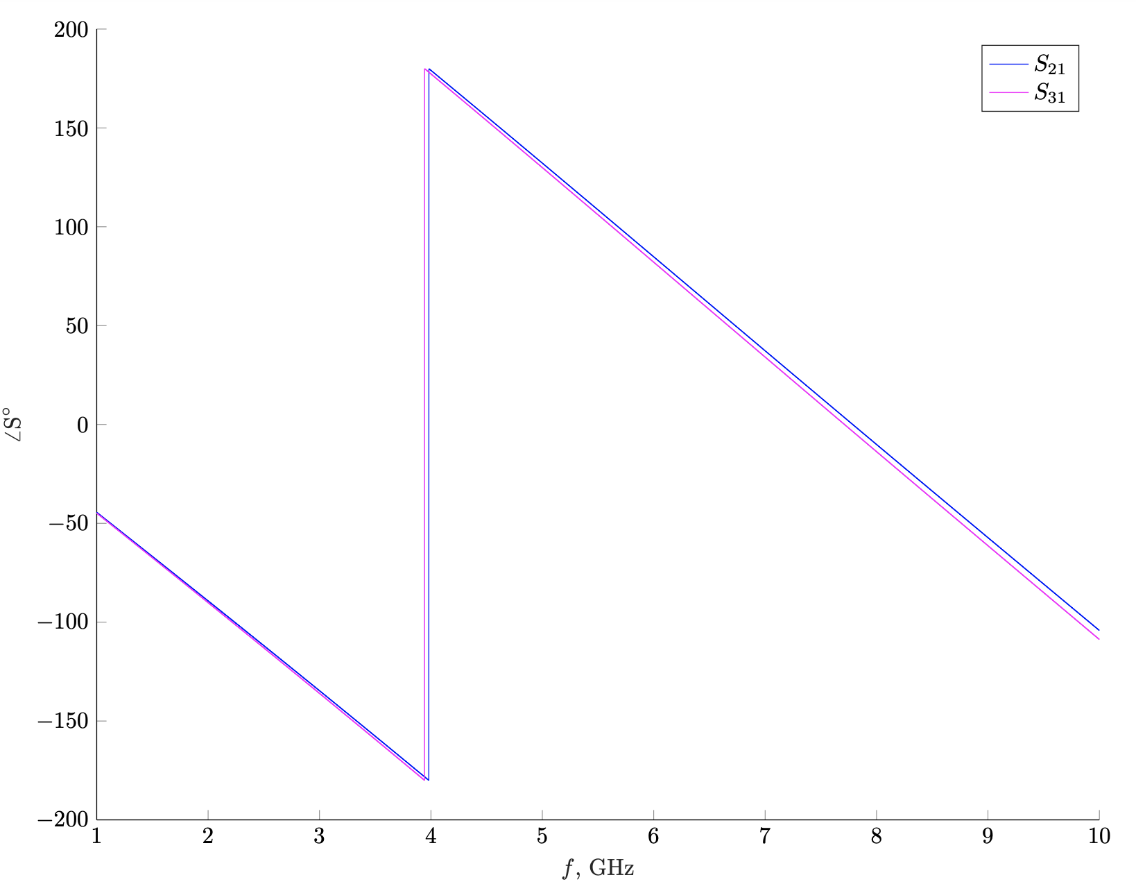 Figure 11 - Module B: Phase difference between $S21$ and $S21$ for the original T-Junction design.
Microstrip Implementation Figure
This system shown in Figure 9 with values from Table 3implemented in microstrip is drawn, the quarter-wavelength section connecting the different ports having a \(90^\circ\) bend in order to reduce parasitic effects. This is a common strategy in microstrip implementations, as in large distributed element systems operating at high frequencies, parasitics greatly influence system behavior.
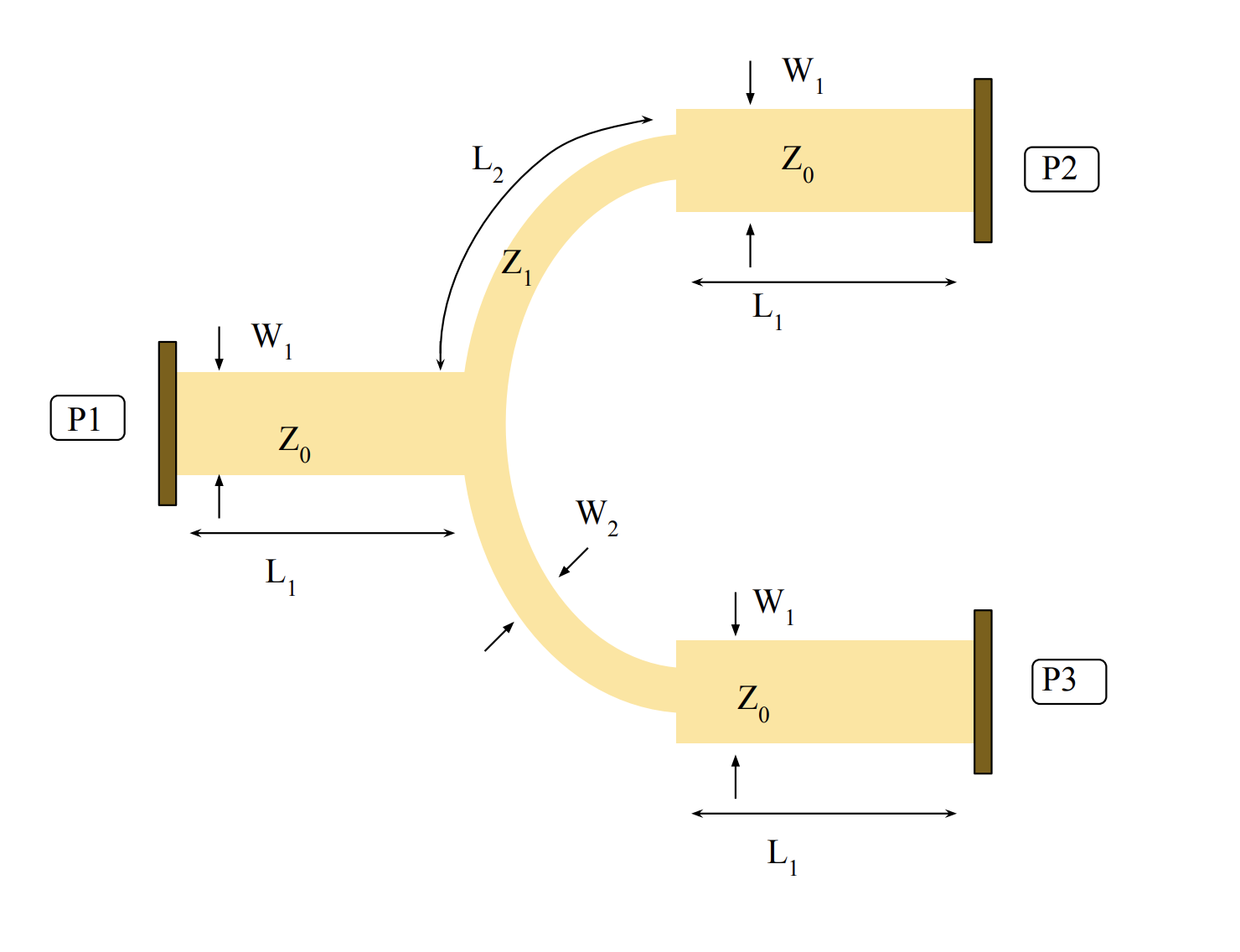 Figure 12 - Module B: Microstrip implementation of T-Junction power divider. (P1 = Port 1, P2 = Port 2, etc.)
Module C: IQ Power Coupling Network
This module implements the quadrature hybrid coupler, a four-port network which evenly divides power to the output ports with a \(90^\circ\) phase difference between them. This is unlike the T-Junction power divider in Module B, which is a three port network that splits signals in phase. These phase shifted signals are sent to the mixers to perform IQ modulation. In addition to this, power sent into an incident port experiences no reflection due to input matching, and no power is delivered to a given port, which is known as isolation.
Quadrature Coupler Design
A schematic for the quadrature hybrid coupler is laid out in Figure 13:
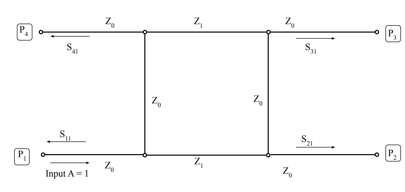 Figure 13 - Module C: Circuit schematic of a quadrature hybrid coupler.
The scattering matrix for this coupler has the following form:
\[\mathbf{S}=\frac{-1}{\sqrt{2}}\left[\begin{array}{cccc} 0 & j & 1 & 0 \\ j & 0 & 0 & 1 \\ 1 & 0 & 0 & j \\ 0 & 1 & j & 0 \end{array}\right] \tag{2}\]From the S-Parameters of the quadrature coupler, we can see the nature of the output phase differences. For example, when port 1 has power sent in, it is equally split to port 2 and port 3. Port 2 has a $90^\circ$ phase difference from port 3. Additionally, we see that port 4 is isolated, and port 1 has no reflection. This same behavior occurs no-matter which port has power delivered to it, however, the output ports and isolated port change. This implies that the system is reciprocal, which we can see from the transpose symmetry of \(\mathbf{S}\) in equation 1. Additionally, since the network does not have resistors or other lossy components, it is lossless. This means that \(\mathbf{S}^H\mathbf{S}= \mathbf{U}\), where \(\mathbf{U}\) is an identity matrix.
This quadrature hybrid has an operating frequency of \(f_0 = 5.95\) GHz and system impedance \(Z_0 = 50\:\Omega\). Carrying out the calculations for the proper widths, lengths, and impedance’s using ADS linecalc, the following system parameters were generated:
| Design | \(\textrm{Z}_0, \: \Omega\) | \(\textrm{Z}_1= \textrm{Z}_0\sqrt{2}\:\Omega\) | \(\textrm{W}_1\), mm | \(\textrm{W}_2\), mm | \(\textrm{L}_1\), mm | \(\textrm{L}_2 = \lambda/4\), mm |
|---|---|---|---|---|---|---|
| Original | 50 | 70.71 | 2.891 | 0.940 | 7.534 | 7.363 |
| Optimized | 50 | 70.71 | 2.891 | 0.940 | 9.798 | 5.775 |
Quadrature Hybrid Validation
The quadrature hybrid shown in Figures 13 and 16 with values from Table 4 was implemented in ADS and simulated over a suitable frequency range of \(1\) to \(10\) GHz to analyze the behavior of the system near the design frequency of \(f_0 = 5.95\) GHz. The device was once again implemented using MTEE, MSTEP, and MBEND components in order to simulate the junction parasitics of the system. The following figure was generated for both original and optimized designs:
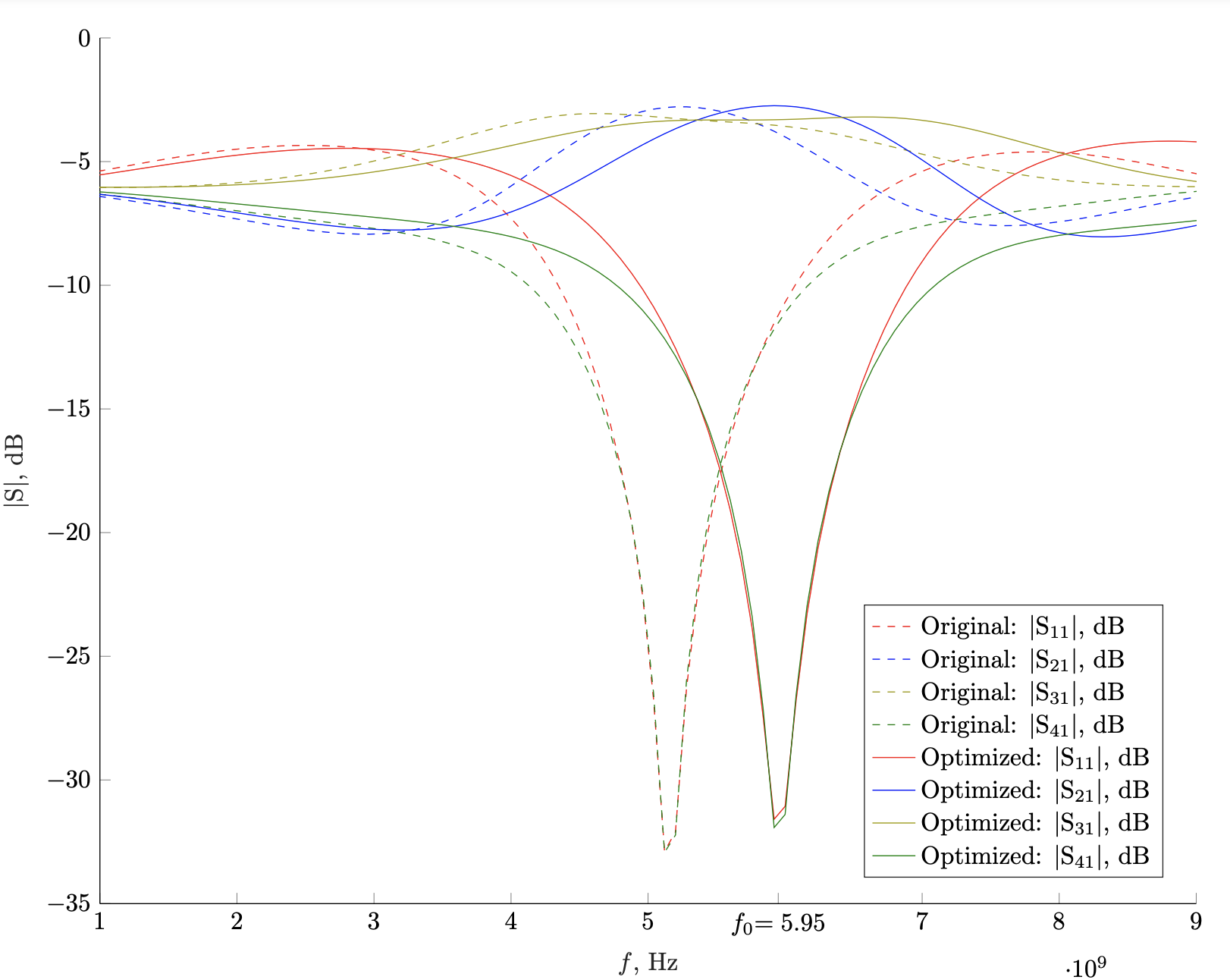 Figure 14 - Module C: S-Parameters for the original and optimized quadrature hybrid coupler designs.
From Figure 14, we can clearly see the expected behavior of the coupler. We see that for the optimized design \(\textrm{S}_{21}\) and \(\textrm{S}_{31}\) achieve close to \(-3\) dB transmission at the design frequency, while \(\textrm{S}_{11}\) and \(S_{41}\) are around to \(-33\) dB since they are matched and isolated, respectively. Figure 14 clearly shows the difference in the original and optimized designs. The original design is once again left of the desired match frequency due to junction parasitics. Allowing the optimizer to change component lengths until desired S-Parameter characteristics are achieved gives a much better system performance with respect to the desired performance parameters. \par The phase of the signals transmitted to ports 2 and 3 must be \(90^\circ\) out of phase, as required by the quadrature hybrid. The S-parameters from Equation 2 indicate that the signal out of port 2 will be \(90^\circ\) out of phase with respect to an input signal at port 1, with port 3 being in phase with the input. This is verified in Figure 15.
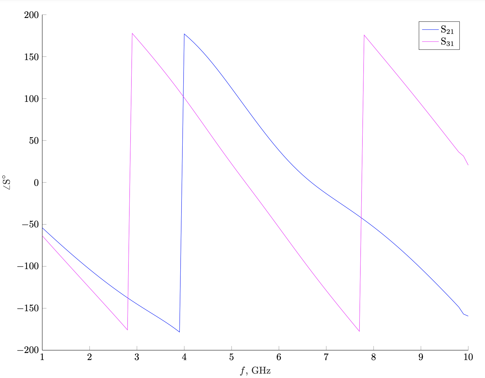 Figure 15 - Module C: Phase (degrees) vs. frequency for \(\textrm{S}_{21}\) and \(\textrm{S}_{31}\) for the original quadrature coupler design.
Microstrip Implementation Figure
The quadrature hybrid coupler of Module C has its microstrip implementation figure laid out here. The junctions are slightly bent to account for parasitic effects, as shown at the corners of each intersection in Figure 16.
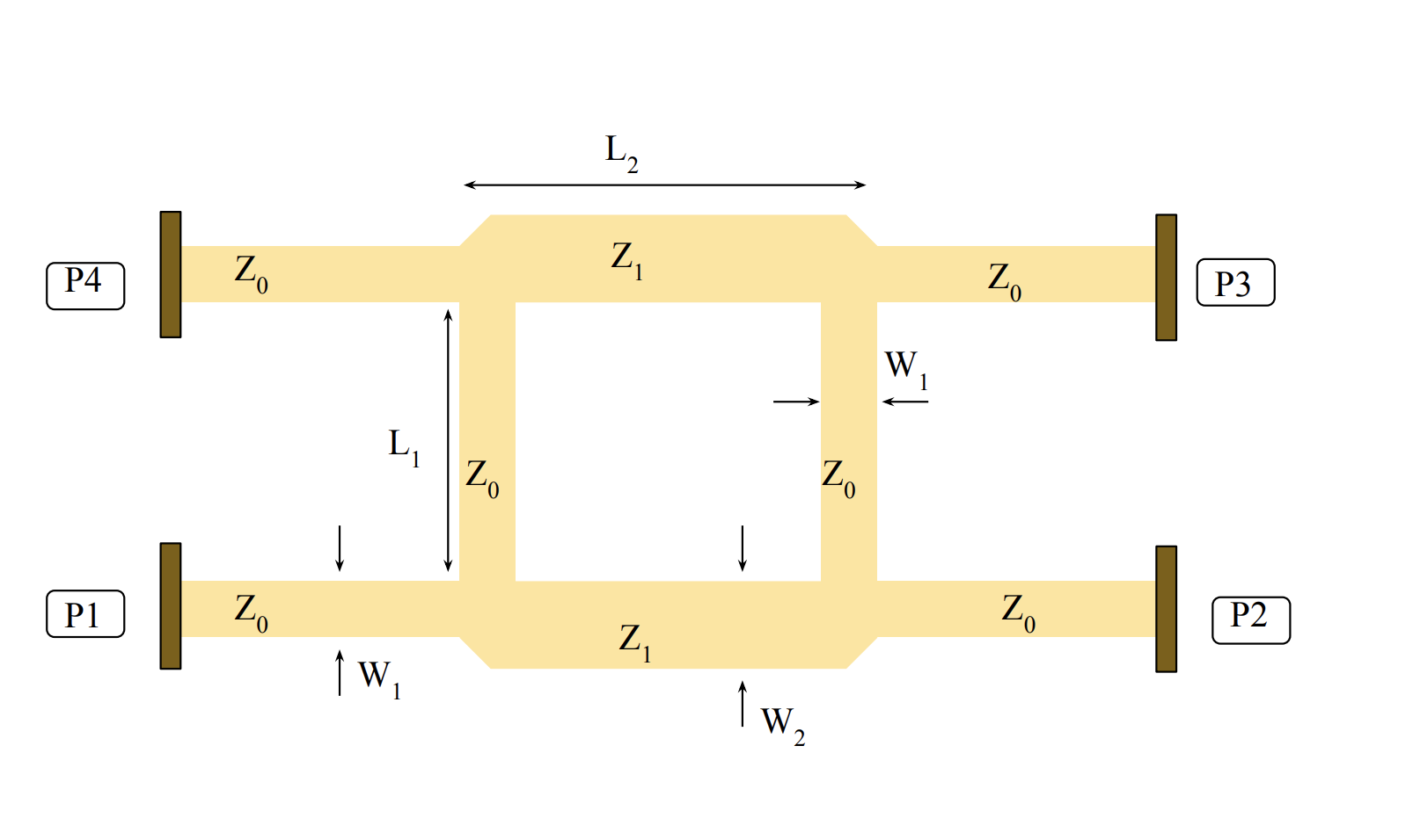 Figure 16 - Module C: Microstrip implementation of a quadrature hybrid coupler. (P1 = Port 1, P2 = Port 2, etc.)
Module D: Matching Network
The LO from the system block in Figure 1 has an output impedance of \(\textrm{Z}_{L} = 100 - \textrm{j}120\) and needs to be matched to the nominally \(50\:\Omega\) input impedance of Module C by a matching network. The matching network can be implemented in either lumped elements or microstrip. This matching network was chosen to be implemented in microstrip since the frequency of operation (\(f_0 = 5.95\) GHz) is sufficiently high, so the distributed element network will be rather small. Additionally, lumped components suffer from tolerance errors (see Module A), and inductors are known to be lossy at high frequencies which will inhibit the performance of the matching network.
Matching Network Design
The matching network design was carried out by hand using a smith chart, and then tuned/optimized using the ADS Tuner and Optimizer. The normalized load impedance \(\textrm{Z}_L = 100 - \textrm{j}120\) was found to first need a transmission line of electrical length \(\beta L_1 = 50.0^\circ\) to rotate to the inverted \(1+\textrm{j}x\) circle. From here, a shunt short circuit stub supplying negative reactance with electrical length \(\beta L_2 = 30.46^\circ\) is used to match the load to the system impedance \(Z_0\). Figure 17 shows a circuit level schematic of this implementation, with associated values found in Table 5.
Once again, parasitic effects are considered in the simulation setup. This leads to resonant frequency of the system to be off from the design value of \(f_0\) by quite some margin. As such, the lengths are first tuned using the ADS Tuning tool to get good \(\textrm{S}_{11}\) matching agreement. After this, the optimizer is configured in order to ensure \(\textrm{imag}(\textrm{S}_{11}) = 0\) at \(f_0\).
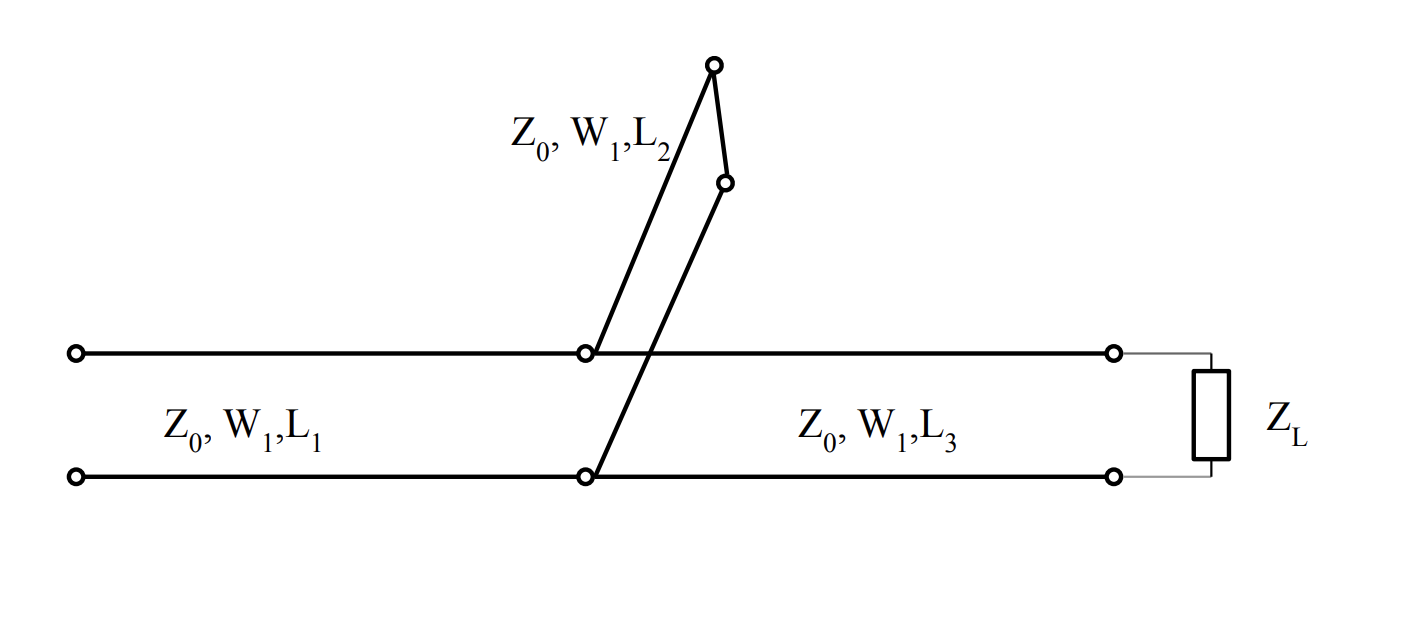 Figure 17 - Module D: Circuit implementation of short circuit stub matching network.
| Design | \(\textrm{Z}_0,\:\Omega\) | \(\textrm{W}_1\), mm | \(\textrm{L}_1\), mm | \(\textrm{L}_2\), mm | \(\textrm{L}_3\), mm |
|---|---|---|---|---|---|
| Original | 50 | 1.725 | 7.534 | 2.550 | 4.185 |
| Optimized | 50 | 1.725 | 8.729 | 2.466 | 3.661 |
Matching Network Validation
The circuit from Figure 17 with values from Table 5 is implemented in ADS using microstrip elements with lengths calculated from linecalc and electrical length derived from smith chart analysis. Simulating \(\textrm{S}_{11}\) over frequency gives insight into the performance of the matching network and is shown in Figure 18.
 Figure 18 - Module D: \(|\textrm{S}_{11}|\), dB vs. frequency for original and optimized matching network designs.
From Figure 18, it is seen that the optimized design has a much better match at the design frequency than the original design. Additionally, the \(-10\) dB fractional bandwidth (FBW) of the optimized design is found to be \(\textrm{FBW} = 22.18\%\). This is fairly wide-band for single-element matching network.
To verify that resonance of the optimized design occurs at the design frequency, the data is visualized in the smith chart format. Figure 19 gives the optimized \(\textrm{S}_{11}\) vs. frequency behavior, clearly showing resonance occurring at $f_0$.
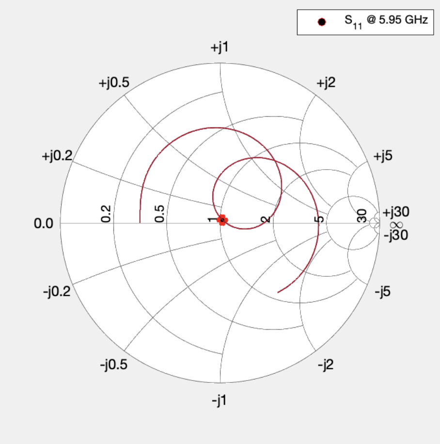 Figure 19 - Module D: Smith chart \(\textrm{S}_{11}\) over frequency for optimized matching network designs.
Microstrip Implementation Figure
The single-element short circuit stub network implemented in microstrip is extremely simple and only requires three transmission line components, each with the same widths but different lengths. It is shown in Figure 20, with corresponding values obtained from Table 5.
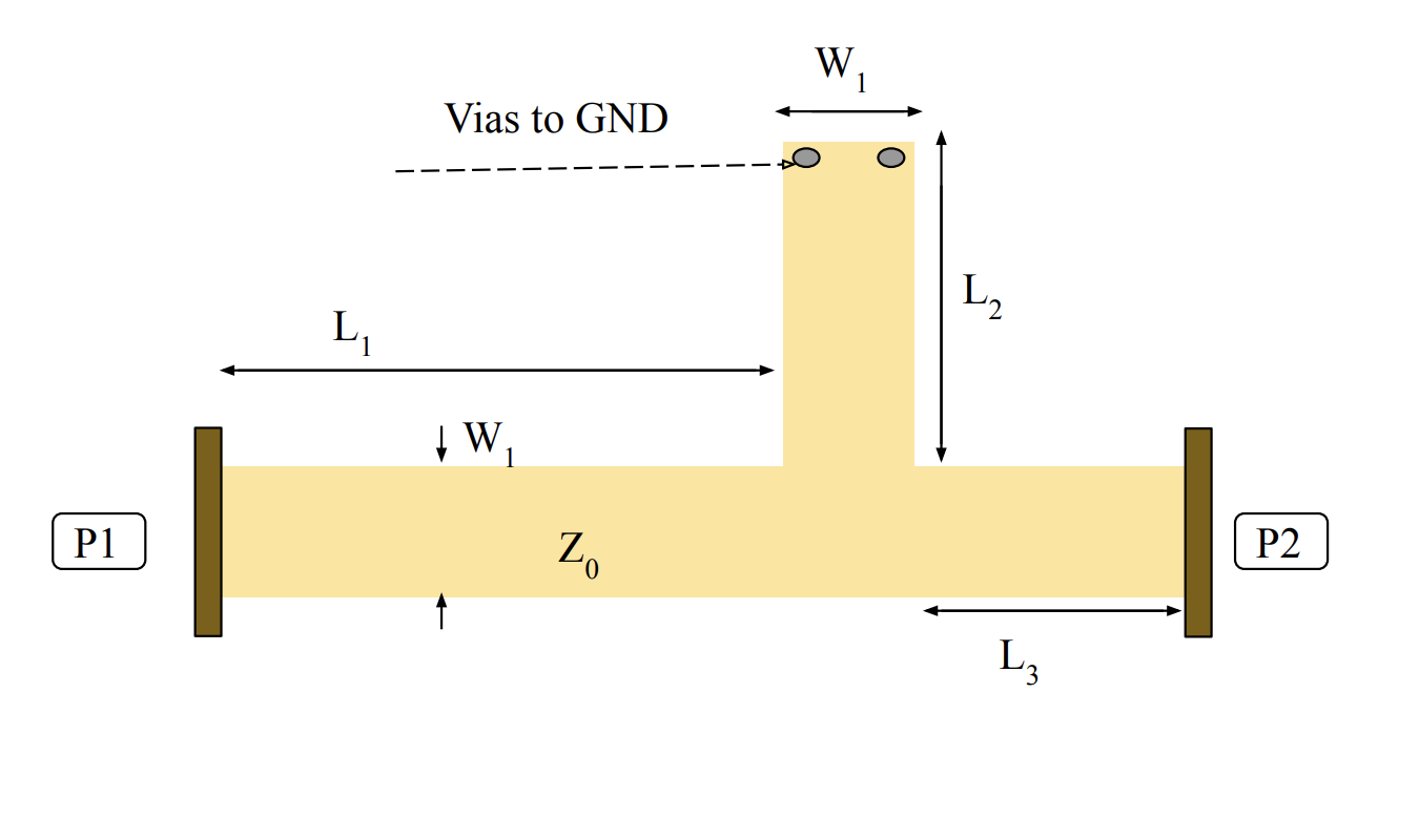 Figure 20 - Module D: Microstrip implementation of short-circuit stub matching network (P1 = Port 1, P2 = Port 2)
Module E: Low-Pass Filter
A low-pass filter is required to filter the output of each mixer with a cutoff frequency of \(0.25\) GHz such that the attenuation at \(0.65\) GHz is \(60\) dB. It is specified that the filter order should be chosen for minimal size based on required filter order while maintaining less than \(2\) dB ripple in the passband.
This module can be implemented in either lumped elements or microstrip. A common implementation of low-pass filters in microstrip utilizes alternating sections of high and low characteristic impedance lines to mimic the behavior of series inductors and shunt capacitors seen in the low-pass prototype (see Figure 2). These are known as stepped-impedance low-pass filters, and they are popular due to their simple design process, and they have the advantage of taking up less space then similar low-pass filters implemented with stubs. That being said, a lumped element low-pass filter is chosen over a stub filter and stepped-impedance filter for this design for a number of reasons. First, the frequency of operation for this module is \(f_0 = 0.25\) GHz which causes the required microstrip segments to have lengths that are on the order of a couple of inches. With the steep attenuation requirement of this design, this implementation would take up a lot of space and is impractical in a system where size is limited. Additionally, distributed element filters have a slower roll-off in the stopband than lumped element filters, so the \(60\) dB attenuation requirement is harder to meet.
Low-Pass Filter Design
The low-pass filter design is carried out in a similar manner to the bandpass filter of Module A. First, a \(0.01\) dB ripple Chebychev filter is selected for this design. Second, a required filter order of \(\textrm{N} = 7\) is needed to realize \(60\) dB attenuation at \(f = 0.65\) GHz. After this was decided, the appropriate normalized low-pass component values were selected to realize a low-pass prototype, which was then frequency and impedance scaled. The circuit schematic for the low-pass filter is given in Figure 21.
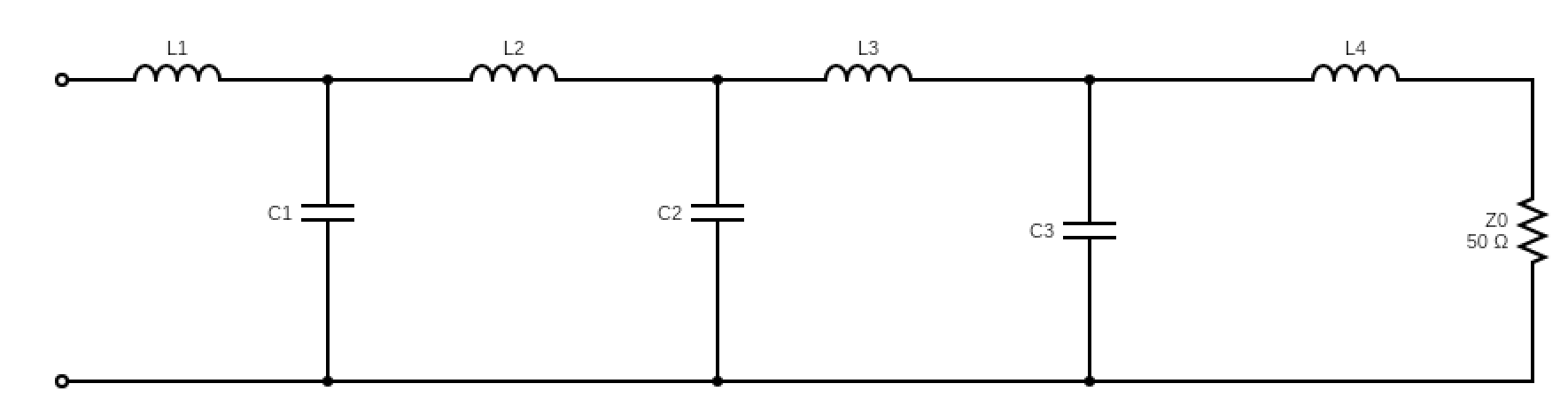 Figure 21 - Module E: Circuit schematic for 7th order Chebychev \(0.01\) dB ripple lowpass filter.
| L1, nH | C1, pF | L2, nH | C2, pF | L3, nH | C3, pF | L4, nH |
|---|---|---|---|---|---|---|
| 25.36 | 17.77 | 55.64 | 20.79 | 55.64 | 17.77 | 25.36 |
No optimization was carried out for this design as the lumped components come extremely close to expected design performance without much of a need to adjust parameters.
Low-Pass Filter Validation
The lowpass filter of Figure 21 with component values from Table 6 is implemented in ADS, and the transmission coefficient \(S_{21}\) of the system is studied to verify system performance. Figure 22 shows the behavior of this low-pass filter:
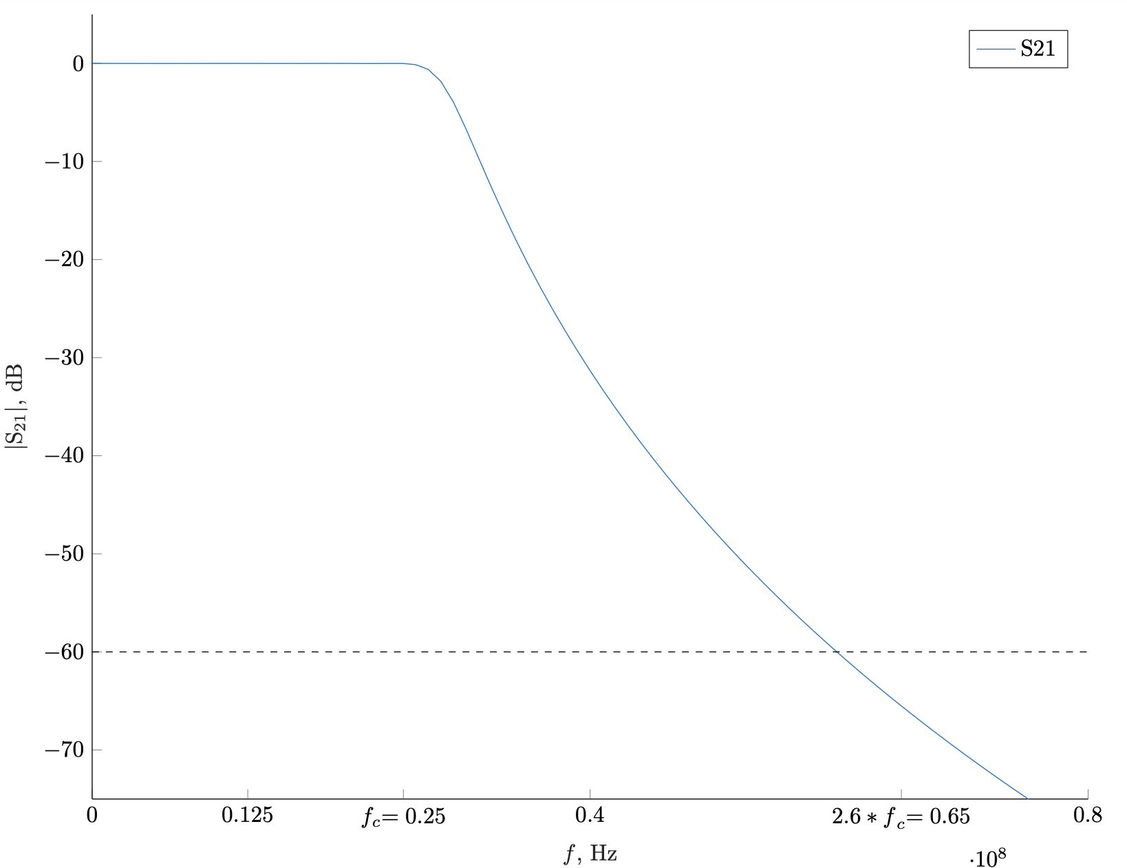 Figure 22 - Module E: \(|S_{21}|\), dB vs, frequency for 7th order Chebychev \(0.01\) dB ripple lowpass filter with cutoff frequency \(f_c = 0.25\) GHz and \(60\) dB attenuation at \(f = 0.65\) GHz}
From Figure 22, the design meets the system performance requirements. The pass-band is extremely flat, as was expected with the choice of prototype values. Additionally, the cutoff is seen at \(f_c = 0.25\) GHz. At \(f=0.65\) GHz, the attenuation is \(-64\) db, which is fairly close to the requirement of \(-60\) dB. Additional optimization routines could easily be run on the lumped component values to achieve \(60\) dB attenuation extremely close to \(0.65\). GHz.
Microstrip Implementation Figure
A lumped-element filter of this type in microstrip would require chip inductors and capacitors. The following diagram in Figure 23 shows how this would look in microstrip, with approximate valid scales accounted for.
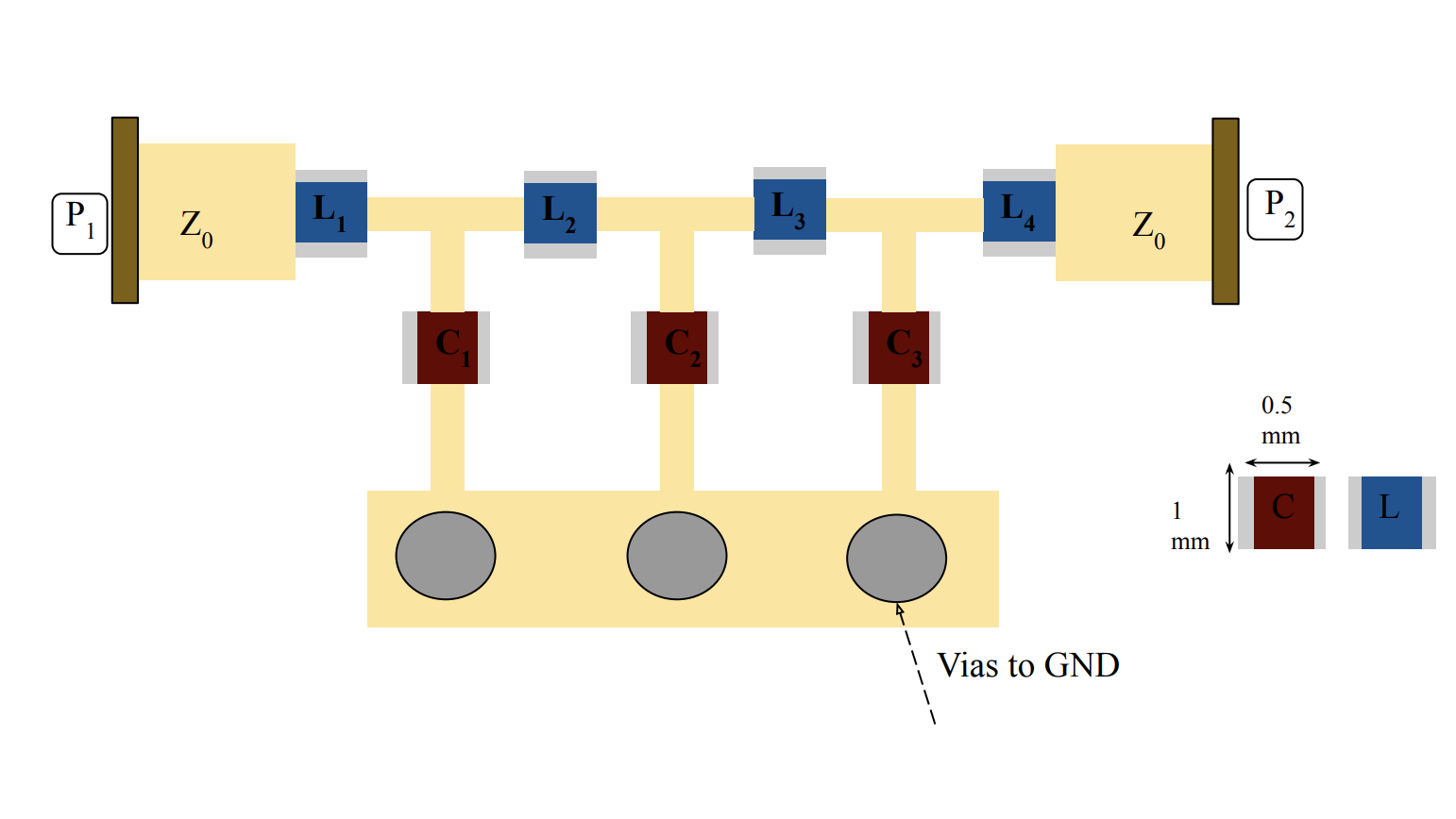 Figure 23 - Module E: Microstrip implementation of 7th order low-pass filter network (P1 = Port 1, P2 = Port 2).
Conclusions
This project was an in-depth exploration into the individual RF modules that constitute an idealized quadrature demodulator. Each module was implemented using either lumped-elements or using microstrip transmission line components, with design selection rationalized and discussed. For each module:
- The selected module element and design processes were explained
- Schematics and tables were provided as a design reference
- ADS simulation was used to verify the designs
- Optimization and tuning was used to refine the design
- A microstrip implementation (to scale) was provided
Additionally, Module A included a section on lumped-element tolerance and the effects it has on the behavior of the system. These effects were subsequently analyzed using Monte Carlo analysis.
Each module provided its own unique insight into the performance of RF systems. Modules implemented using lumped-elements highlighted both the advantages and disadvantages of lumped-element networks. The advantages include easy design, cheap implementation, and relatively small size. The disadvantages of lumped elements include component tolerance and high frequency losses. For microstrip implementations, advantages include small size at high frequencies, ability to realize more reactive values, and lower-loss than lumped-elements at high frequency. Disadvantages of microstrip implementations include potentially more complicated circuit implementations and additional parasitic effects due to microstrip discontinuities.
Overall, this project shows that a designer has many different choices at their disposal when it comes time to design a system. Trade-offs between different implementations and methods must be carefully considered with respect to the design requirements in otder to synthesize a functional, high-performance system.