
For my final year undergraduate project, I worked in a team on an ISM band RF energy harvesting system for powering (very) low energy loads. Despite this project happening during the peak of the COVID-19 pandemic, my partner and I were able to successfully develop and test hardware to prove this concept out in the lab! This post will give an overview and background to RF energy harvesting, describe the problem that RF energy harvesting hopes to solve, present detailed design and test results, and give a roadmap of potential future applications.
 Figure 1 - The many potential applications of RF energy harvesting.
Overview and Motivation for RF Energy Harvesting
The idea of wireless power transfer (WPT) has existed since the rise of modern electrical engineering in the late 19th century. Nikola Tesla was the first to conceive of the usefulness of WPT, declaring the ability to transfer energy without physical connections or wiring as, “an all-surpassing importance to man” 1. However, a limitation of WPT systems are low-input powers, not only making system design difficult, but also restricting its application to specific types of loads.
Fortunately, WPT and radio-frequency energy harvesting (RFEH) are now seen as promising future technology due to recent advances in CMOS technology and the ability to utilize low-input powers in small form-factor devices. The exponential increase in electrical computing efficiency is known as [Koomey’s Law], which states that the number of computations per Joule of energy dissipated doubles about every 1.57 years 2. This trend is visualized in Fig. 2 over the time period of 1940 to 2010.
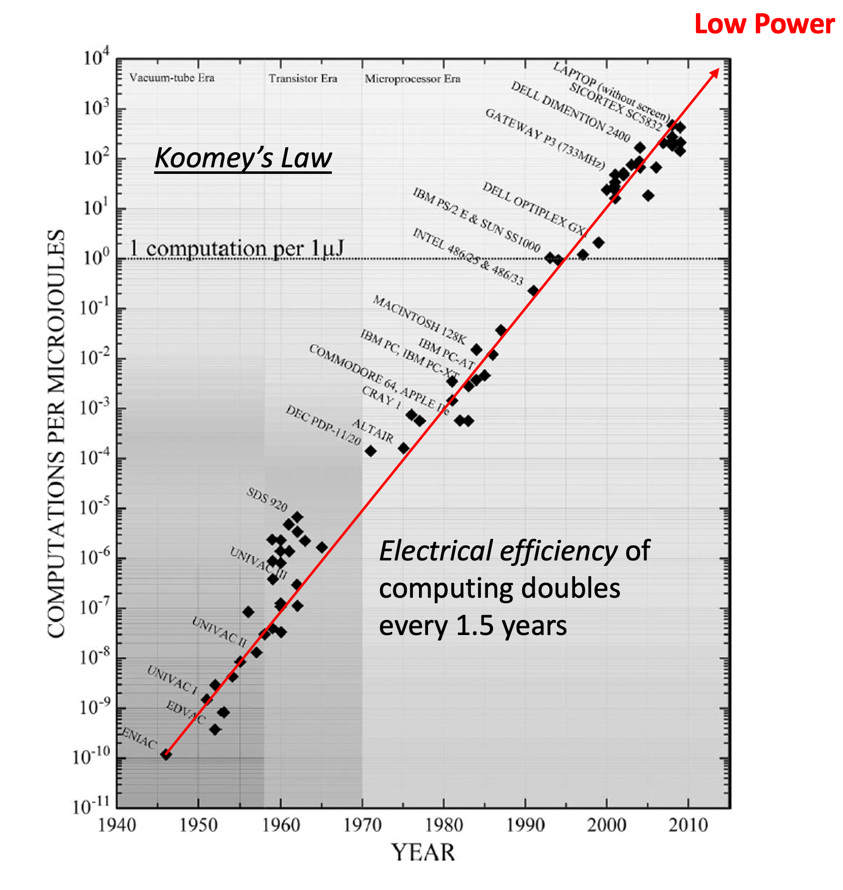 Figure 2 - Number of computations per micro-Joules averaged over an hour. A micro-Joule is the sum of 1-\(\mu\)W power during 1s, or 100 nW during 10s. 2
The trend of increasing computational efficiency indicates a future where many devices will operate with minimal power consumption. As a result, RFEH systems will be able to act as practical power sources for a select class of devices. A potential target application of RFEH are Internet of Things (IoT) devices. In the coming years, IoT low-power sensors are expected to be an ubiquitous technology, and RFEH provides a potentially low-cost and enduring alternative to batteries.
Comprised of large sensor networks connected via communication channels, IoT grids require complex wiring schemes or dedicated batteries at the device level 3. As the world becomes more and more connected, the efficient manufacturing and maintenance of IoT devices will become an urgent matter; by 2030, the number of connected devices is predicted to reach 125 billion 4. Powering these sensor networks via wired power-grid or primary batteries will soon become infeasible due to cabling costs and the finite lifespan of batteries, which require maintenance and replacement. As an alternative solution, energy supplied by dedicated RF sources will allow IoT networks to be powered wirelessly.
Some Technical Aspects
In far-field WPT systems, an antenna and rectifier, abbreviated as rectenna, carries out the process of converting RF input to usable direct current (DC) output. First developed by William C. Brown in the 1960’s 5, rectennas are devices that can supply energy to traditional low-input power applications and theoretically support infinite device lifetime by removing the need for dedicated batteries with a finite energy supply.
The challenge of designing an efficient WPT system is sustaining a high RF-to-DC conversion efficiency, as the system’s efficiency is a function of input power levels, operation frequency, and discrete component properties. These factors change the input impedance of the rectifier network, causing the receive antenna to be mismatched with the rectifier, thus leading to loss of input power and lower conversion efficiency. Therefore, a realized system must be designed with the operating conditions known prior to the physical design. A simplified block diagram of an RFEH system is shown in Fig. 3. Such a system has many components that introduce loss and lower the conversion efficiency from its maximum value of 100 %. Because the input-power levels of the system are already low, significant effort needs to be made to ensure proper impedance matching between components.
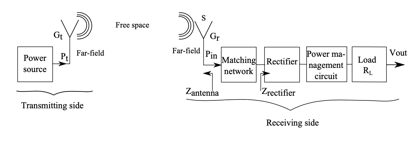 Figure 3 - Block diagram of a far-field WPT system 6. A matching network is utilized to ensure maximum power transfer at the specified operating conditions.
Many of these IoT sensors operate in conditions where it is infeasible, expensive, or dangerous to replace a battery or to deliver wired power. Examples include health monitoring sensors 7,8, structural support sensors 9, aircraft structural monitoring sensors 10, and sensors utilized in hazardous environments. Overall, the requirements for such sensors include:
- Small size
- Low maintenance
- Unknown exact location
This project aims to meet these system requirements in a manner that maximizes system efficiency by carefully designing each component of a WPT network.
A detailed block diagram of the implemented RFEH system is depicted in Fig. 3. The performance parameters which affect system operation are highlighted along with each component. A successful RFEH system attempts to optimize all of these factors simultaneously in order to keep the DC output voltage at a level required by the load application.
The system primarily consists of two elements: the transmitter and receiver. The transmitter has an associated transmit power and carrier frequency, and can either function as an ambient or dedicated source. An ambient source is one that exists for some other purpose, such as mobile broadcast stations or routers used for wireless communications. These sources may have an associated signal modulation scheme which can impact performance. In contrast, a dedicated source is specifically designed to supply power to a select receiver/load side, resulting in higher efficiencies. The transmit antenna can be optimized depending on the target application. For example, a high gain antenna is preferred in situations where the rectenna’s location is known, allowing for the transmit antenna to supply power over a greater distance compared to an omnidirectional antenna.
Between the transmitter and receiver is a free-space region. An energy harvesting system that captures energy sent over a free-space region greater than the far-field distance \(R>2D^2/\lambda\) (where \(D\) is the largest linear dimension of the transmit or receive antenna and \(\lambda\) is the operating wavelength) is classified as a far-field RF energy harvester. The received power levels for a far-field energy harvesting system can be accurately modeled by the Friis transmission equation 11
\[P_{\mathrm{rx}}=P_t\left(1-\left|\Gamma_{t}\right|^{2}\right)\left(1-\left|\Gamma_{r}\right|^{2}\right)\left(\frac{\lambda}{4 \pi R}\right)^{2} G_{t}\left(\theta_{t}, \phi_{t}\right) G_{r}\left(\theta_{r}, \phi_{r}\right)\left|\hat{\rho}_{t} \cdot \hat{\rho}_{r}\right|^{2}, \tag{1} \label{eq:Friis}\]where the received power \(P_\mathrm{rx}\) is a function of the power transmitted (\(P_{t}\)), the matching level of the transmitter and receiver (\(\Gamma_{t}\) &, \(\Gamma_{r}\)), the operating wavelength (\(\lambda\)), the transmitter-to-receiver separation distance (\(R\)), the gain of the transmit and receive antennas (\(G_t\), \(G_r\)), and polarization mismatch between the transmit and receive antennas
\[\left|\hat{\rho}_{t} \cdot \hat{\rho}_{r}\right|^{2}\]On the receive side, the first element is the antenna. The antenna is designed to be low-gain such that it can receive input RF energy from any direction. The antenna operates over a specified bandwidth to capture the incident carrier signal. Additionally, the antenna must be matched to a nominal system impedance to minimize reflection losses and ensure maximum power transfer. In this case, a nominal system impedance of \(Z_0 = 50\;\Omega\) is used.
Likewise, the rectifier needs to be matched to the system impedance. However, challenges arise as the rectifier’s input impedance non-linearly varies as a function of frequency, input power, and load impedance. Thus, a robust simulation model that can capture and represent these effects is crucial for the design of the system.
The output of the rectifier is interfaced with a power management unit (PMU) to store energy and drive the load application. Ideally, the PMU operates in a region that presents a fixed DC resistance to the rectifier, allowing the rectifier to be optimally matched to this value. The load application has its own specifications, such as power consumption and usage period, in addition to minimum driving conditions required for the system to initially be powered.
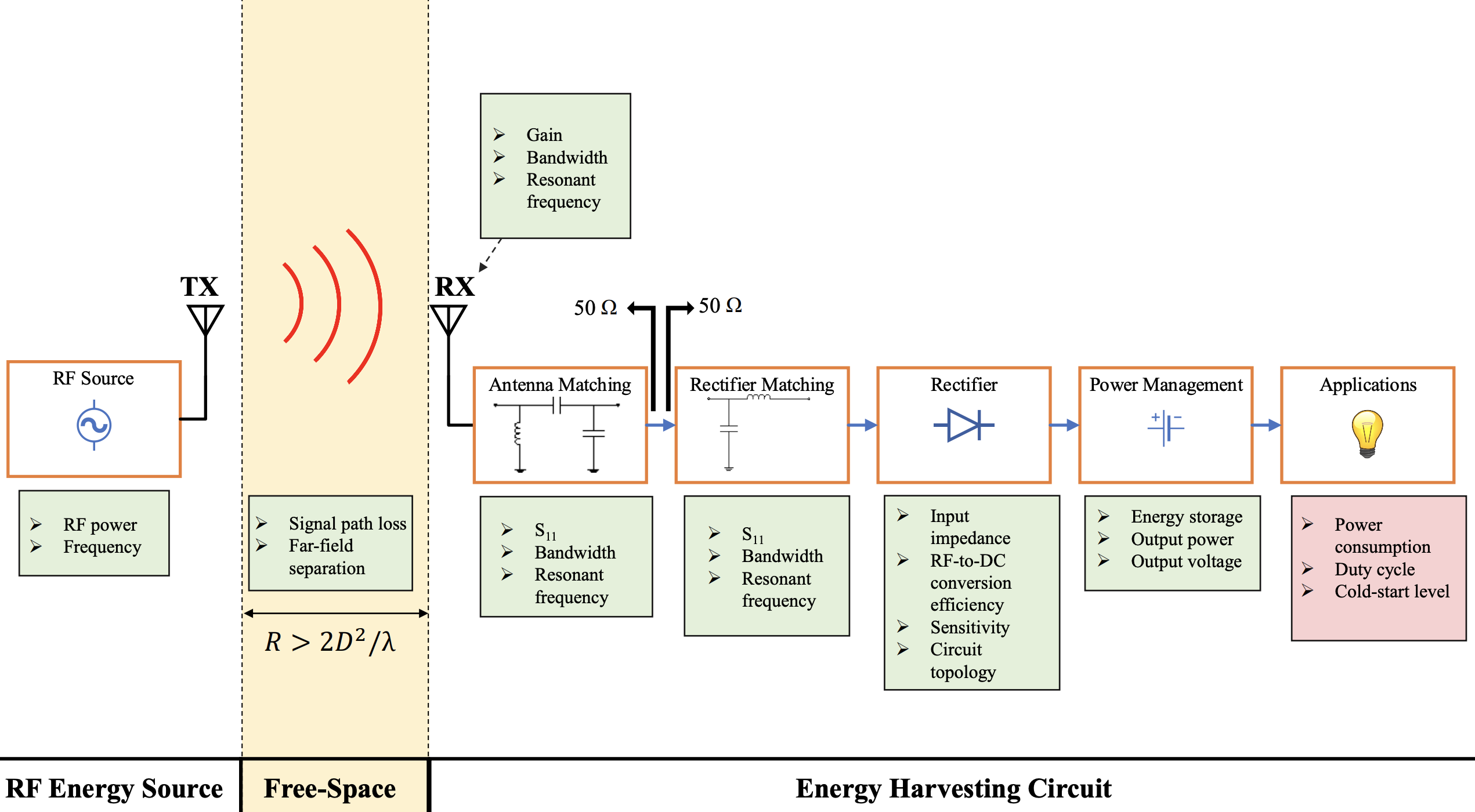 Figure 4 - Block diagram of implemented system.
Some Modern Efforts
Within industry, Powercast Corporation creates various devices powered by far-field RFEH via dedicated power sources [^powercase]. Although their technology also converts RF energy to DC power, their systems operate in the 915 MHz band. On the other hand, our system aims to operate at a higher frequency of \(2.45\) GHz.
Academic researchers have successfully created devices in an effort to expand the field of RFEH. Many of these devices are designed to operate in common frequency bands which do not require special licenses, such as the 2.4-2.5 GHz WiFi ISM band 12,13,14,15,16,17. However, few of these systems are integrated with a sensor load, and if so, they are not tested at the appropriate power transmit level. For example, in 13, a rectenna sensor network designed at 2.45 GHz is tested using a 10 W Effective Isotropic Radiated Power (EIRP); possible sources operating at this frequency (e.g. routers) typically provide a maximum of 4 W EIRP, the maximum limit set by the U.S. Federal Communications Commission (FCC). While this solution proves the feasibility of integrating a sensor network with rectenna, it does not adequately imitate a practical environment.
Current efforts either:
- Omit validation of their system via integration with a practical application
- Lack an accurate sense of how a rectenna-sensor network would fare in realistic conditions
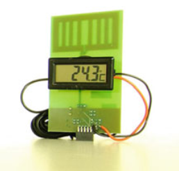 Figure 5 - Rectenna integrated with temperature system operating at 915 MHz 3.
With current research in mind, our project aims to create a rectenna system that operates at \(2.45\)~GHz as an effort towards developing feasible power sources for IoT sensors. Our project will further advancement by not only designing the rectenna system, but also proving it can power commercial, low-power integrated circuits and IoT sensors in a realistic environment. Note that due to technical challenges and time constraints, many simulations and tests are done at the frequency $2.1$ GHz (see Section Design Changes later in the post).
Project Overview
Design Approach
The project’s design methodology was comprised of a three-phase plan. The first phase consisted of a detailed literature review, along with initial system layout and component selection. The next phase involved simulations of the various sub-components and the integrated system as a whole. The final phase was fabrication and measurement, in which expected simulation results were validated using various RF measurement devices.
Simulations
Much of this work depends on simulations that approximate the behavior of an RFEH system operating in real-world conditions. Advanced simulation tools are required to characterize the rectifying circuit and design the receive antenna. A non-linear circuit simulator utilizing the Harmonic Balance technique 18 is used to characterize the rectifier network, as the junction capacitance of the diode as well as the physical device properties require careful analysis for efficient matching network design (see Fig. 6). This technique partitions a nonlinear circuit, i.e. a rectifier containing diodes, into non-linear and linear sub-components. The linear subcircuit is analyzed in the frequency domain, while the non-linear subcircuit is analyzed in the time domain, after which the results are Fourier transformed to the frequency domain. The currents through nodes separating the sub-circuits are “balanced” at each harmonic, and from this, the corresponding input impedance can be determined for each frequency contained in the system. This tool was used to quantify the rectifier network’s input impedance at the fundamental frequency $f_0$ and the chosen average input power level. Additionally, this circuit simulator was used to view the generated DC output level in order to estimate RF-to-DC conversion efficiency for various input powers.
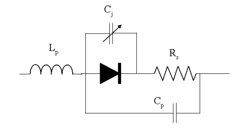 Figure 6 - Equivalent circuit of a packaged diode]{Equivalent circuit of a packaged diode can be analyzed using Harmonic Balance. \(\mathrm{L_p}\) is the packaging inductance, \(\mathrm{C_p}\) is the packaging capacitance, \(\mathrm{R_s}\) is the series junction resistance, \(\mathrm{C_j}\) is the junction capacitance 19.
Simulation of the receive antenna took place after the characterization of the rectifier network. This simulation utilized Ansys HFSS, a 3D full-wave electromagnetic solver, in order to accurately design and tune the antenna before fabrication. Once the antenna was fully characterized using numerical tools, the S-parameters of the system were extracted in order to generate a circuit representation of the antenna. This data was then used to simulate the rectifier and antenna in one system. The antenna can be directly matched to the complex conjugate of the input impedance to the rectifier at the fundamental frequency \(f_0\) for a fixed power level \(P_{\mathrm{in}}\) and load \(R_\mathrm{L}\). Alternatively, both networks can be matched to a nominal system impedance \(Z_0\). The latter matching method is the approach taken in this design, although the former method may lead to marginally higher power conversion efficiency levels due to lower parasitic component losses.
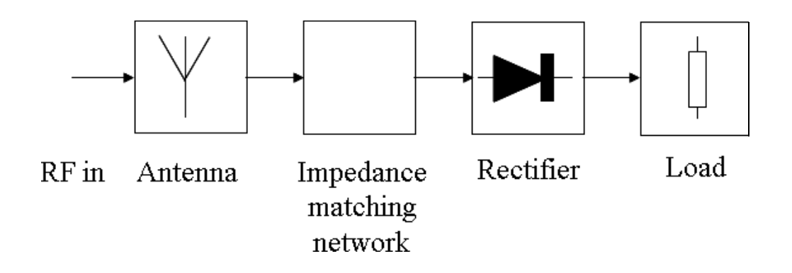 Figure 7 - Block diagram of an integrated rectenna system. After the rectifier/load network has the input impedance characterized for a specific RF power input, an impedance matching network can be designed and placed between the antenna and rectifier 19.
System Design & Components
This section will cover the design, simulation, and measurements of each individual component in the finalized RFEH system.
Antenna
The receive antenna was designed to both capture incident power densities and present an input impedance close to the system impedance \(Z_0\) at the design frequency \(f_{0}\). Many different antenna topologies can be utilized in RFEH systems, however, with one of the primary system objectives being a low-profile geometry, a planar microstrip based antenna was selected as the antenna type. Microstrip antennas have a simple initial design process, which can then be tuned to achieve certain performance results such as polarization diversity or dual-band operation 11. Additionally, microstrip antennas can utilize various feed networks, allowing for various system layout configurations, and can be efficiently integrated onto a PCB sharing analog and digital circuitry.
The antenna topology chosen for the final design was the planar inverted F antenna (PIFA). The PIFA consists of a rectangular planar element placed above a ground plane, a short-circuit pin, and a microstrip feed. The PIFA layout used in HFSS simulations is depicted in Fig. 8.
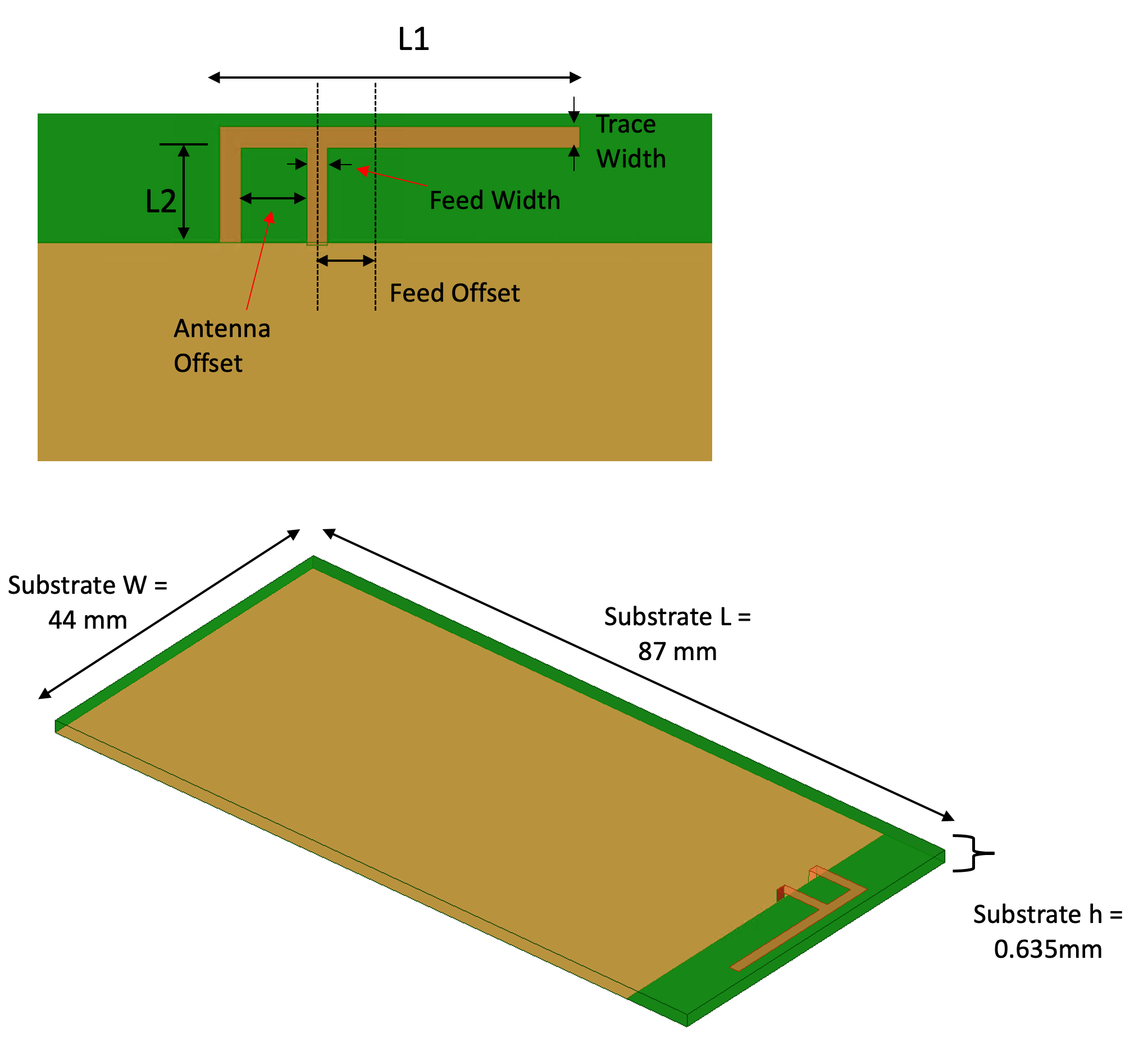 Figure 8 - PIFA geometry and PCB dimensions.
| L1 mm | L2 mm | Ant. Offset mm | Feed Offset mm | Feed Width mm | Trade Width mm |
|---|---|---|---|---|---|
| 22.5 | 8.47 | 3.9 | 4.5 | 1.2 | 1.3 |
The PIFA is a variant of a standard monopole antenna, where the top section has been folded to be parallel to the ground plane, effectively creating the image of a dipole. This also reduces overall antenna height while maintaining a length required for resonance. The arm denoted by length \(L_\mathrm{1}\) forms a shunt capacitance to ground, which is inductively tuned by the short-circuit stub of length \(L_\mathrm{2}\).
The ground plane plays a crucial role in the operation of the PIFA. Exciting currents in the PIFA causes excitation of currents in the ground plane. The radiated electromagnetic field is a result of the interaction between the PIFA and its image below the ground plane. The radiation performance is dependent on the geometry of the ground plane, and is typically enhanced when the ground plane is much greater than the dimensions of the antenna itself. In general, the width of the ground plane should be at least as wide as the PIFA \(L_\mathrm{1}\) arm, while the length should be at least \(\lambda/4\) in height 11, where \(\lambda\) is the free-space wavelength at the operating frequency.
The dimensions of the PIFA are listed in the table below Fig. 8. The resonant frequency of the antenna is determined by the lengths of the radiating arm, shorting pin, and trace width, and the location of the feed relative to the shorting pin 11. The resonant frequency is specified such that \(L_\mathrm{1}+L_\mathrm{2}+\left(\mathrm{Trace\;Width}\right) = \lambda/4\) at \(f_0\). In this case, \(\lambda\) is the free-space wavelength at $f_0$. These values are fine-tuned using the Optometrics tool in HFSS to get an optimal resonant behavior at $f_0$. The initial design frequency used in all the simulations is \(f_0 = 2.45\) GHz, however this value can be adjusted by means of a matching network (i.e. \(f_0 = 2.1\) GHz), as it is for the final system implementation discussed in later sections.
The numerically tuned antenna is simulated in HFSS to characterize its directivity and efficiency, as measuring these parameters in a lab requires extremely specialized equipment and highly controlled test environments which were not accessible for this project. As seen in Fig. 9, the gain of the antenna is fairly omnidirectional with a peak gain of $3.7$ dBi. This gain value is used in theoretical link-budget calculations involving the fabricated design as this parameter was not able to be characterized without an anechoic chamber.
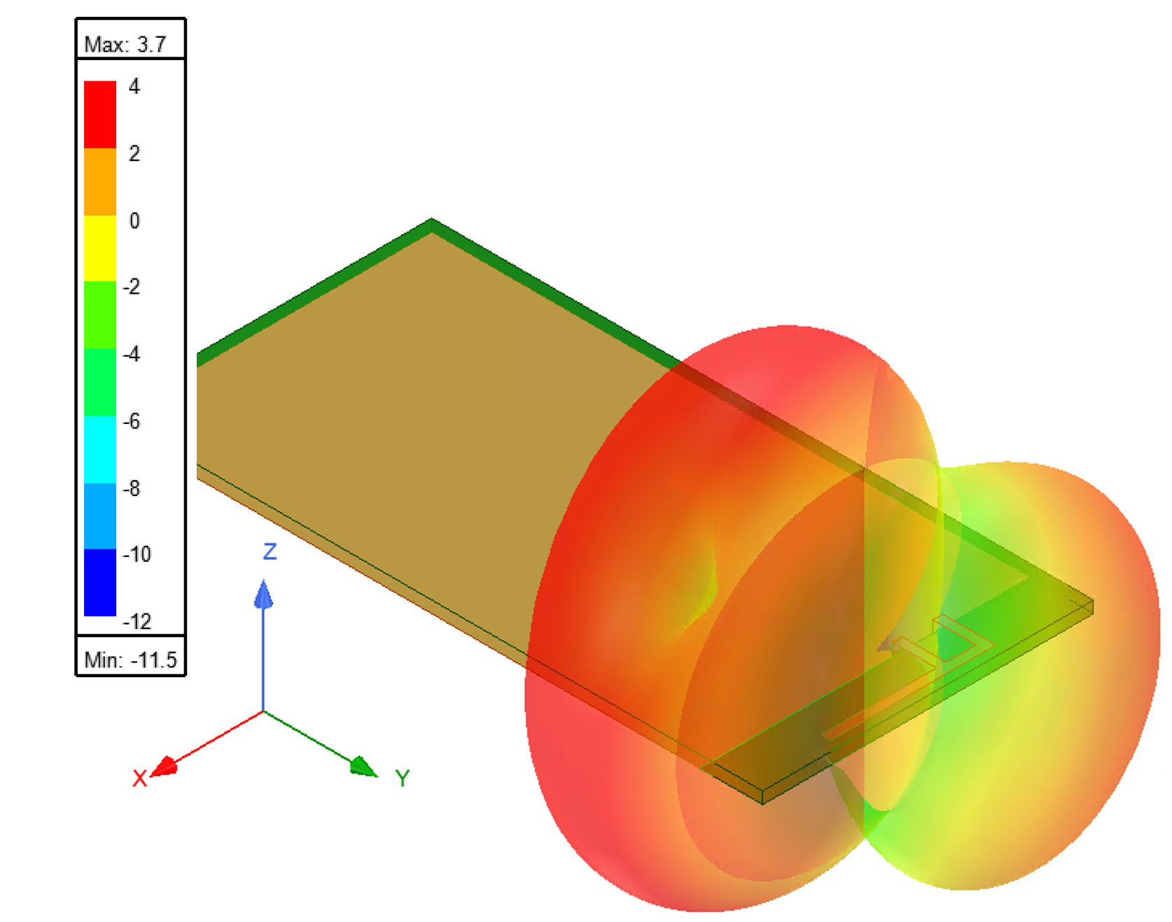 Figure 9 - Simulated PIFA gain pattern.
The measured PIFA is tuned to an operational frequency of \(f_0 = 2.1\) GHz by means of a \(\pi\)-topology matching network. The lumped component values along with the reflection coefficient \(S_{11}\) response of the system is depicted in Fig. 10.
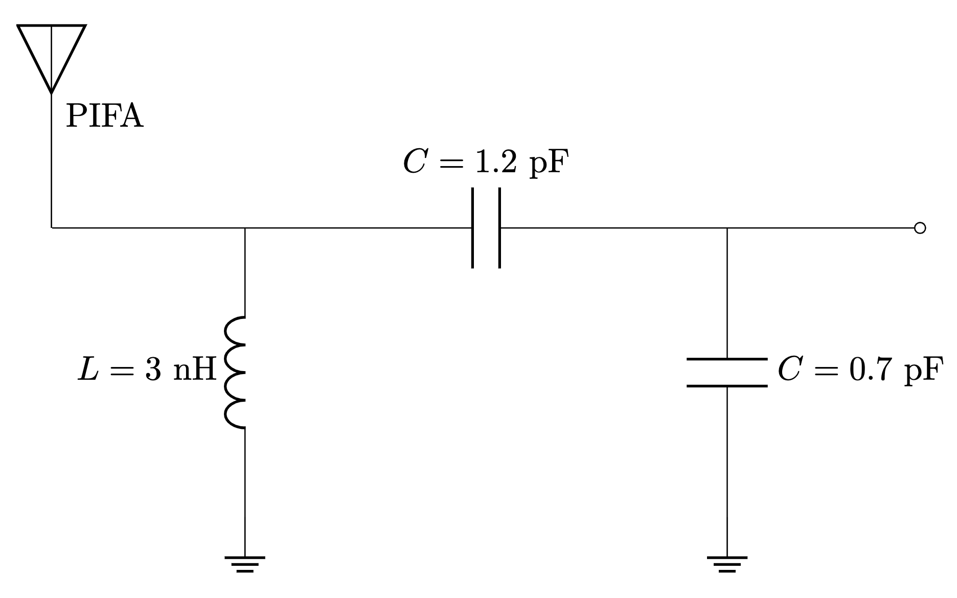 Figure 10 - Antenna matching network (top) and S11 response depicted by Smith chart (bottom left) and log-magnitude plot (bottom right).
| Smith Chart | Log Magnitude |
|---|---|
 |
Rectifier
The rectifier is responsible for converting an input AC signal to a DC output that can then be used to power application-specific loads. In order to ensure maximum power transfer between the antenna and rectifier, reflection should be reduced and the rectifier should be matched to the system impedance, i.e. \(Z_0 = 50~\Omega\). A voltage doubler circuit, shown in Fig. 11, and an input power of -10 dBm were chosen based on their prevalence in RFEH literature 3, 20, 15, 13. Here, \(\mathrm{Z_{source}}\) denotes where the matching network will be placed, which is implemented to match the fundamental frequency’s input impedance to the nominal system impedance \(Z_0\) for a specific input power and load resistance.
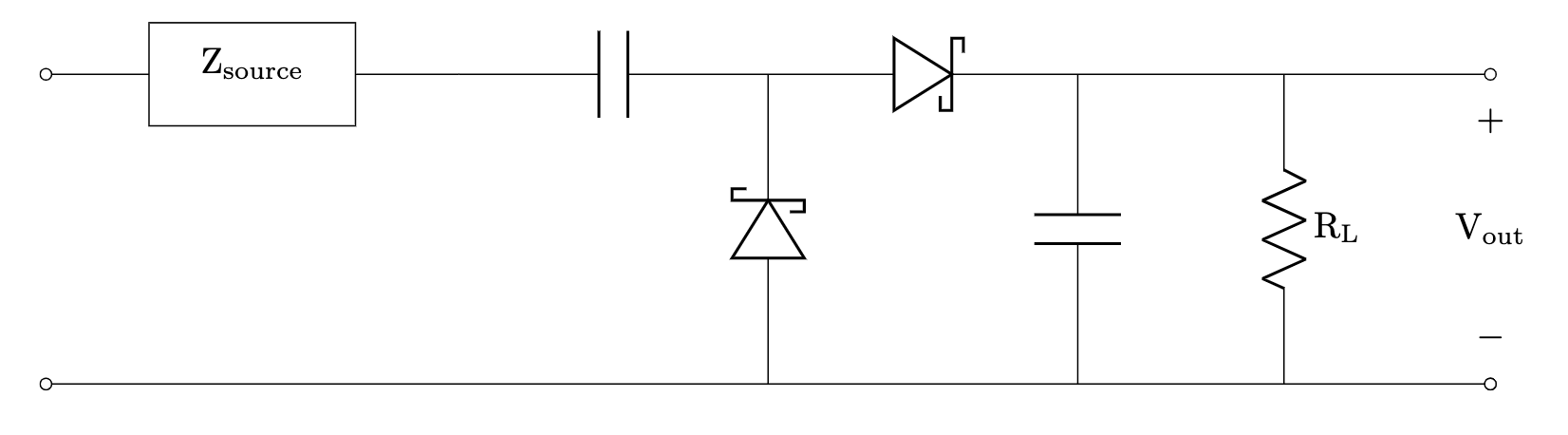 Figure 11 - Grenaicher voltage doubler circuit consisting of Schottky diodes, capacitors, and load resistance.
The rectifier’s impedance was analyzed using large-signal s-parameter (LSSP) simulations and Harmonic Balance solvers in ADS software. The rectifier circuit is matched at 2.1 GHz, with matching components obtained through ADS optimization and physical tuning (see Fig. 12 for component values and Fig. 18 for \(S_{11}\) response).
Due to the non-linear nature of the diode, the rectifier performs differently as the input power and load resistance vary. The effects of input power and load resistance on efficiency are visualized in Fig. 13. The graph shows that a maximum efficiency of 30% occurs with input powers between \(-5\) to \(0\) dBm, with a load resistance less than 5 k\(\Omega\). Ideally, the rectifier would operate in this region of maximum efficiency.
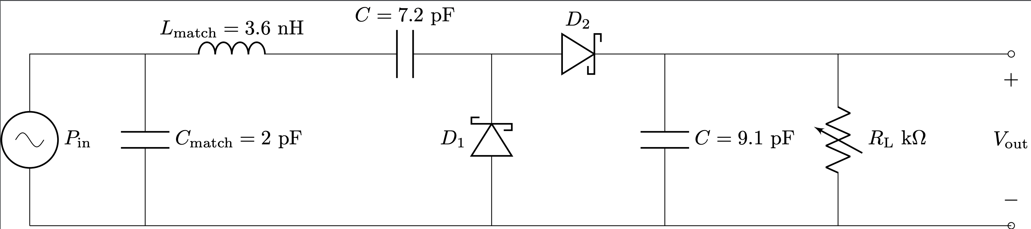 Figure 12 - Matched rectifier circuit with variable input power and output load control.
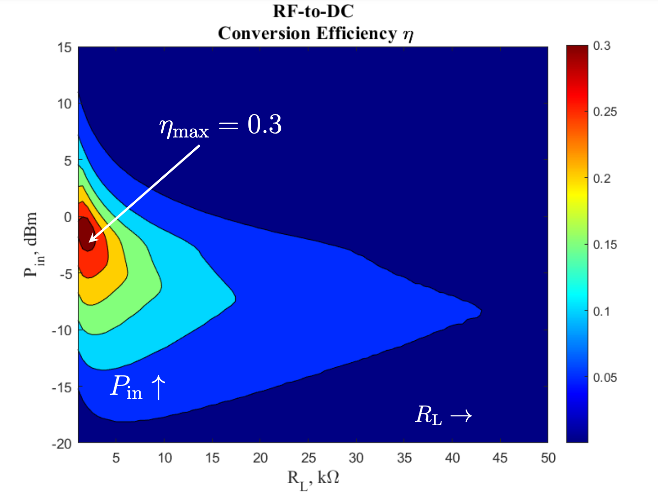 Figure 13 - Simulated contours of efficiency as a function of load resistance and input power.
PCB: Integrated Rectenna
The designed antenna and rectifier elements detailed in the previous sections were integrated onto a common PCB substrate and fabricated in order to conduct system-level tests and validate the design concept. Altium designer was used for both the schematic capture and PCB layout of the design (see Fig. 14 and 16). As seen in Fig. 15, the fabricated PCB area is confined by the dimensions used to simulate the PIFA antenna in HFSS (refer to Fig. 7).
Lumped components, i.e. Murata GCM15 capacitor and LQW15 inductor, synthesized the matching networks and rectifier. These components are rated for radio-frequency operation and have high component Q-factors, leading to minimal component losses and thus enhancing power conversion efficiency 21. The diodes used in the rectifier are the SMS7630-040LF by Skyworks 22. This particular series is a Schottky diode, which is essential for RFEH applications as they have the lowest turn-on voltage, are self-biasing, and have fast switching speeds. Additionally, this diode was selected due to its low junction capacitance of \(C_{\mathrm{j0}} = 0.14\) pF, relatively low parasitic series resistance of \(R_\mathrm{s} = 20\;\Omega\), and minimal packaging parasitic inductance and capacitance.
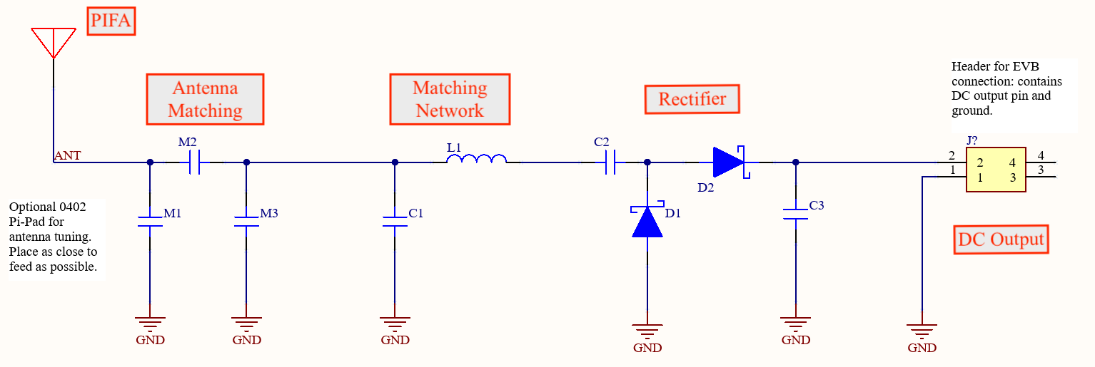 Figure 14 - Custom rectenna schematic; designed in Altium.
Via shielding was added to enhance isolation between the antenna and rectifier, as well as to reduce parasitic inductance on the board. From a measurement standpoint, a top-layer ground is required in order to have a properly grounded RF probe connected to the PCB for characterization. The table below Fig. 16 details the substrate parameters of the board. The board uses Rogers 6006 dielectric 23, which was chosen based on its permittivity and substrate height such that trace widths of characteristic impedance \(Z_\mathrm{0} = 50~\Omega\) can smoothly interface with 0402 surface mount components, thereby minimizing parasitic stub effects on the board. Additionally, this substrate is very low loss and has consistent material properties, resulting in designs that more accurately reflect the simulations.
At the output of the rectifier are additional solder pads for connecting a \(1\times 2\), \(1.27\) mm pitch header in order to interface with a standalone PCB containing the power management IC and digital temperature sensor.
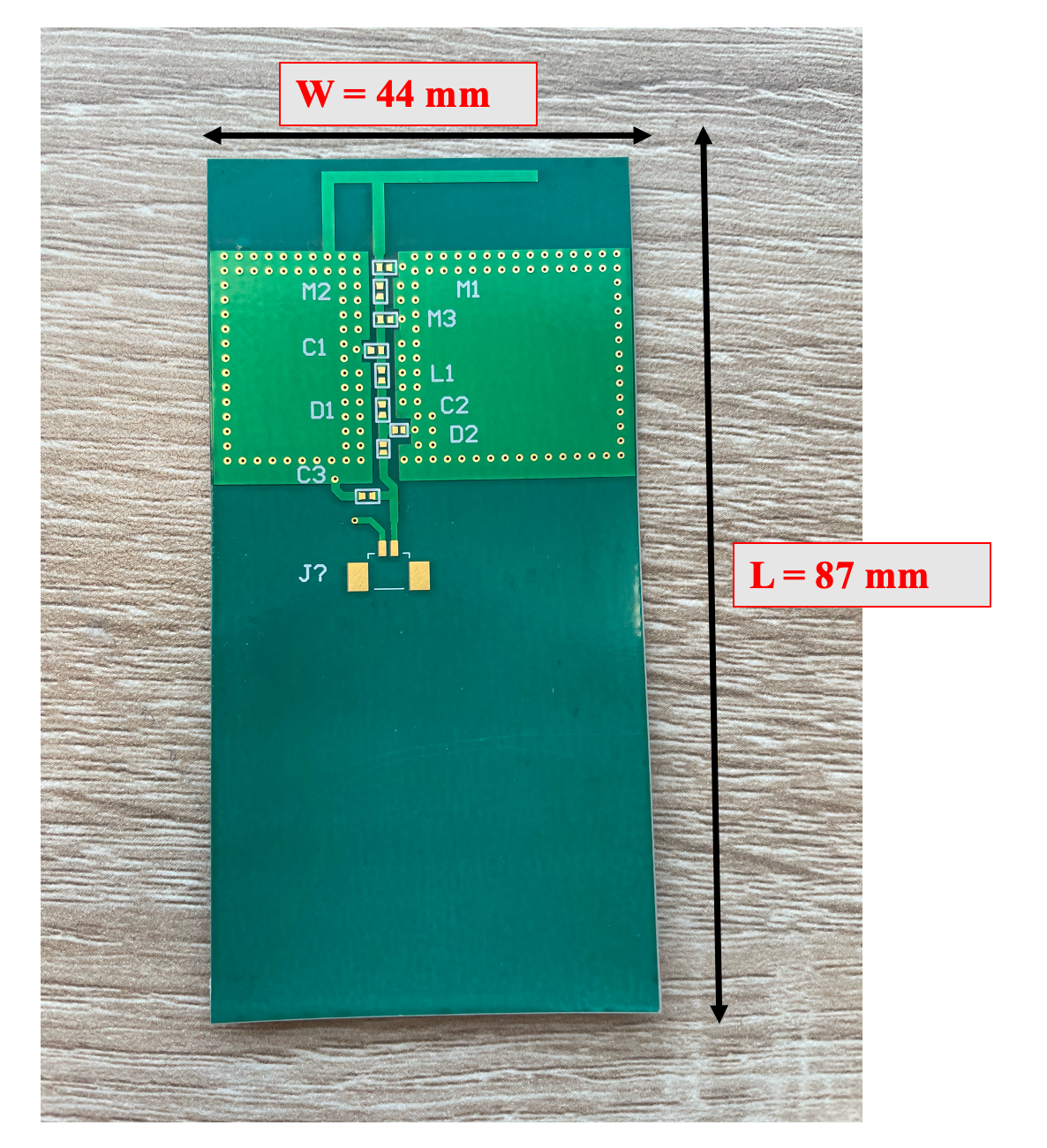 Figure 15 - Fabricated PCB.
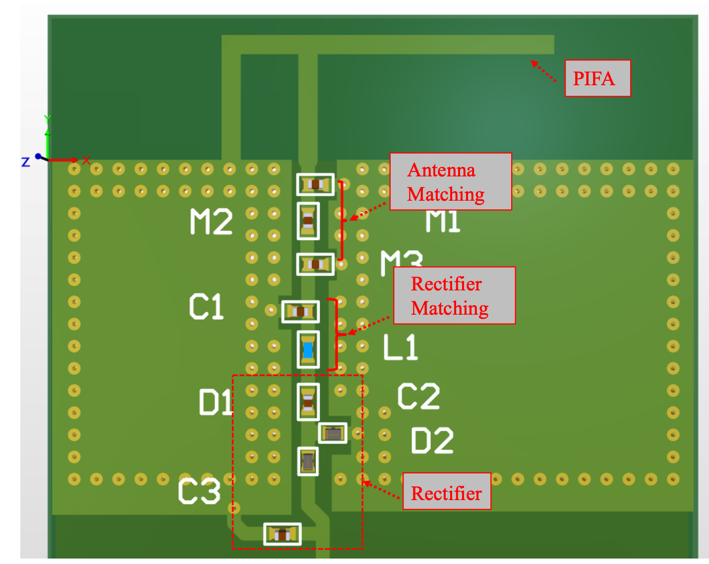 Figure 16 - Altium layout.
| Substrate | Permittivity \(\mathbf{\epsilon_\mathrm{r}}\) | Dielectric Height _hD | Trace Width $w$ |
|---|---|---|---|
| Rogers 6006 | 6.15 | 0.635 mm | 0.935 mm |
System Testing
In this section, the measured performance of the system is presented. First, the rectifier is characterized by soldering a \(50\;\Omega\) probe directly to the rectifier and its matching network in order to control the power supplied to the circuit. Multiple experiments are run in this way to characterize the rectifier to observe how its behavior aligns with ADS simulations. Next, over-the-air (OTA) testing is performed utilizing the receive antenna as well as a dedicated RF power source. The rectified output voltage is characterized as a function of incident power density, and theoretical link-budgets are carried out to model the transmitter-to-receiver path loss.
Rectifier Performance
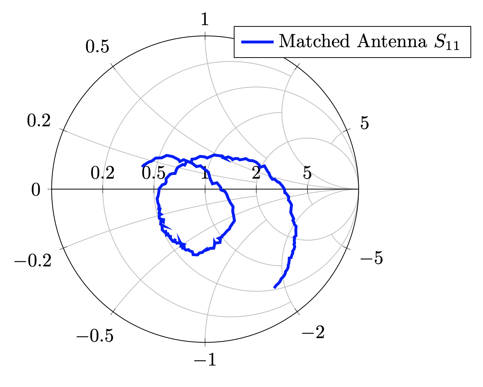
Extensive testing of the fabricated rectifier board was carried out in order to validate the physical PCB against the simulated expectations. The first test carried out was a measurement of the rectifier’s input impedance at the fundamental frequency $f_0$ when presenting a \(50\;\Omega\) source impedance to the circuit. The simulated and measured results of the rectifier with \(R_{\mathrm{L}} = 10~\mathrm{k}\Omega\) and \(P_{\mathrm{in}}=-10~\mathrm{dBm}\) are plotted on a Smith Chart in Fig. 17. Both simulation and measurement align well, indicating that the simulation model of the board and components is robust.
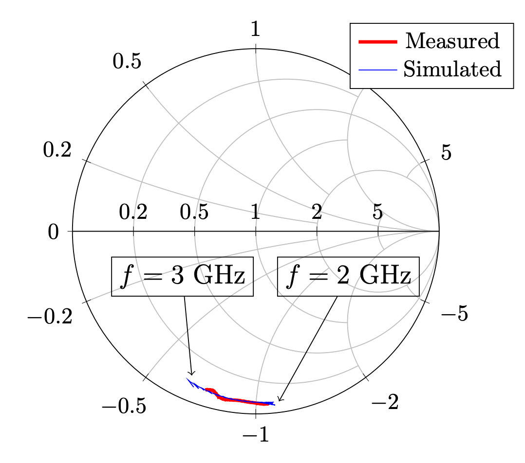 Figure 17 - Smith Chart plotting simulated and measured results of the unmatched rectifier from 2 to 3 GHz.
For designing/verifying the performance of the rectifier’s matching network and power conversion efficiency, the board was modified as shown in Fig. 18. A \(50~\Omega\) RF probe was soldered to the top ground of the PCB to connect a VNA or RF signal generator in order to directly interface with the rectifier.
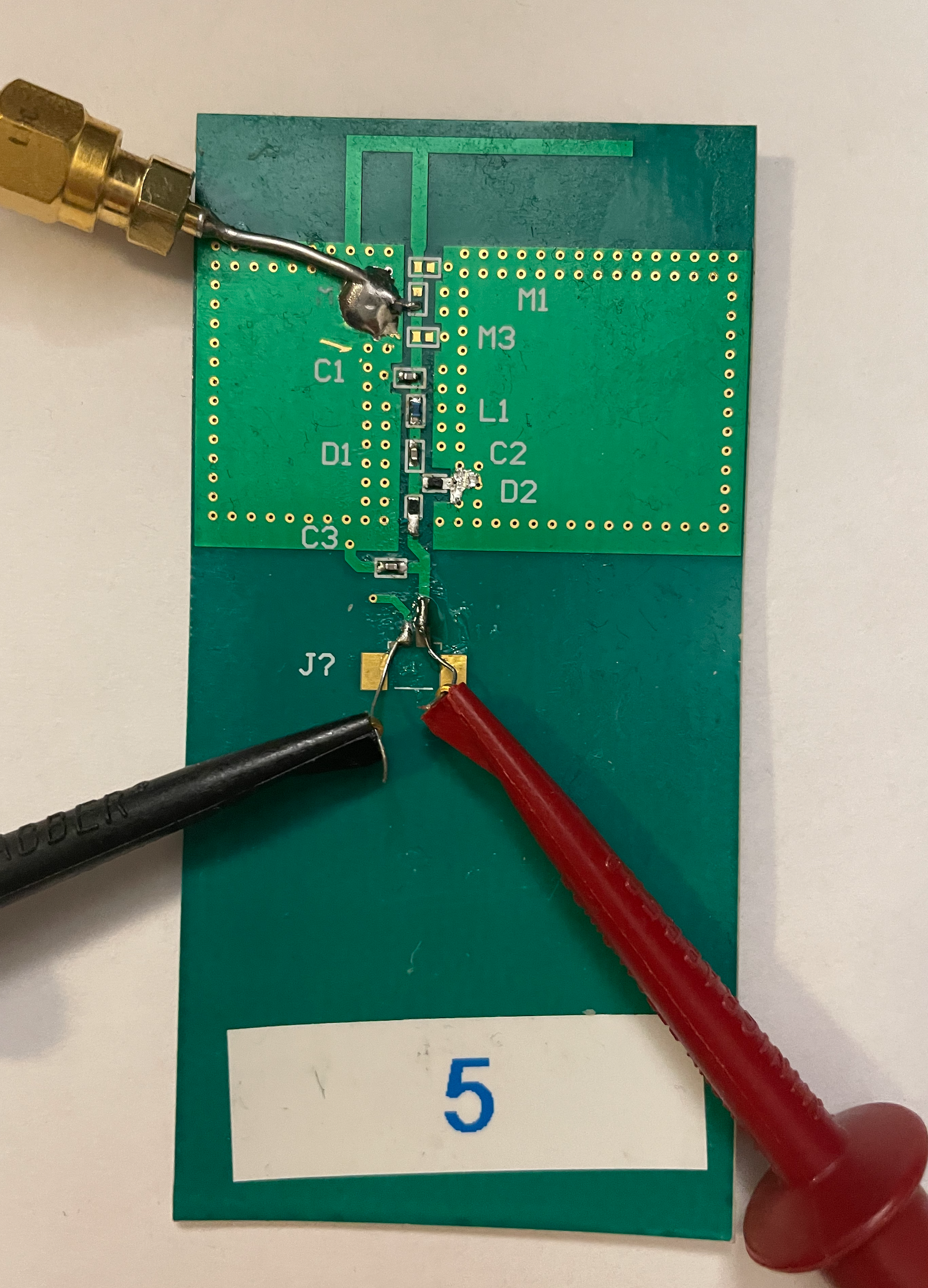 Figure 18 - Test setup for matching rectifier and characterizing the conducted response. A \(50~\Omega\) RF probe is soldered to the top ground of the PCB. This is used to interface with a vector network analyzer or signal generator depending on the test.
Using the measured input impedance data along with ADS optimizations of matching network topologies, a suitable matching network is designed for a fundamental frequency of \(f_0 = 2.1\) GHz. The resulting matching circuit topology and lumped element values along with the \(S_{11}\) response is shown in Fig. 19.
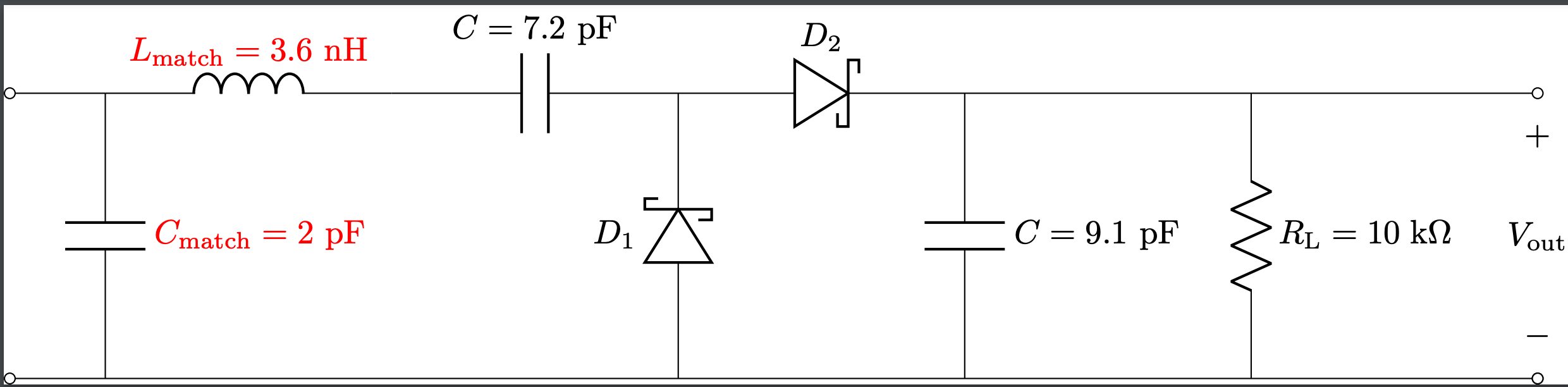
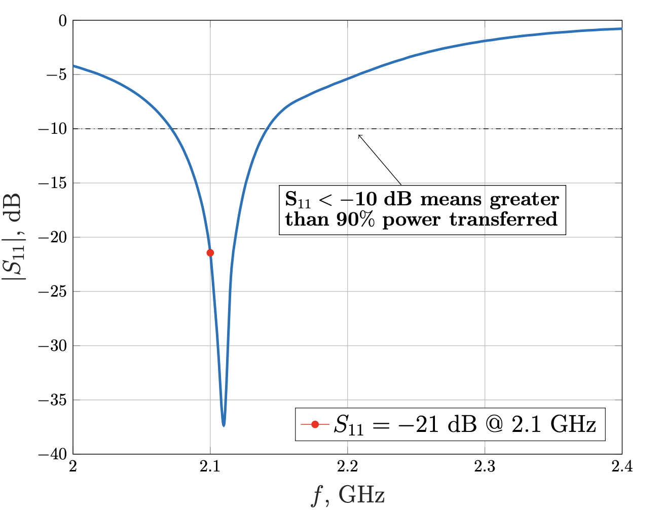 Figure 19 - Matched rectifier circuit (top) and \(S_{11}\) response for fixed input power \(P_{\mathrm{in}}=-10\) dBm, \(R_\mathrm{L}=10~\mathrm{k}\Omega\) (bottom).
After successfully matching the rectifier on the PCB, the output voltage is characterized as a function of load resistance for different input powers. The test setup consists of an RF signal generator to control the input power and frequency, the rectifier, jumpers to a breadboard, a potentiometer to control the load resistance, and a digital multi-meter to record output voltage levels. The setup is shown in the top of Fig. 20.
The bottom of Fig. 20 shows the simulated and measured output voltage versus load resistance at different power levels. From the plots, it is clear that the physical board aligns closely with the simulations. Analyzing the trends of these curves, one can see that, for low load resistances below \(3~\mathrm{k}\Omega\), low output voltages are produced. This is important when integrating with the PMU, as the IC must present an effective DC load resistance high enough to ensure that operation conditions are satisfied. It is also observed from the curves that above a certain value, increased load resistance does not result in higher output voltage levels.
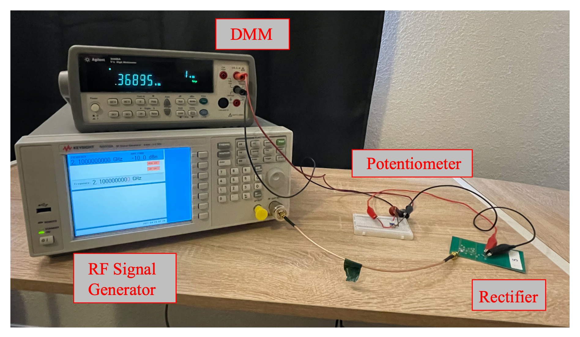
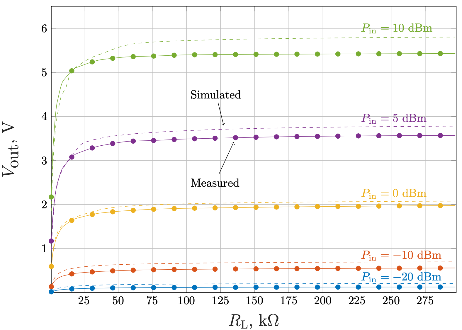 3 Figure 20 - Test setup for characterizing the rectifier (top) and output voltage \(V_{\mathrm{out}}\) as a function of load resistance \(R_\mathrm{L}\) for different input powers \(P_{\mathrm{in}}\).
Finally, we characterize the power conversion efficiency \(\eta_{\mathrm{\scriptsize PCE}}\). The power conversion efficiency is defined as the amount of DC output power \(P_\mathrm{DC}\) attained with respect to the RF input power \(P_\mathrm{in}\),
\[\eta_{\mathrm{\scriptsize PCE}} = \frac{P_{\mathrm{DC}}}{P_{\mathrm{in}}} = \frac{V_{\mathrm{out}}^{2}}{R_\mathrm{L}\cdot P_{\mathrm{in}}} \tag{2}\]We observe general agreement between the behavior of simulation and measurement, however our measurements likely have increased component losses, leading to lower overall efficiency as seen in Fig. 21.
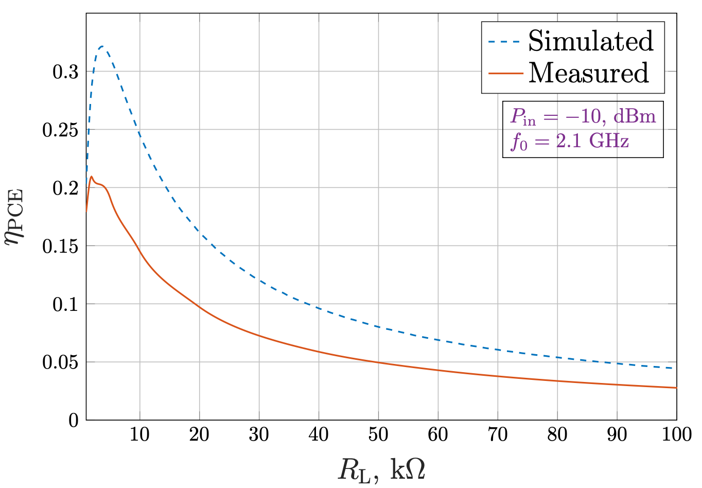 Figure 21 - Simulated and measured power conversion efficiency as a function of load resistance \(R_\mathrm{L}\) for a fixed input power \(P_{\mathrm{in}}=-10\) dBm and frequency \(f_0=2.1\) GHz.
Over-the-Air Performance
After independently validating the performance of the rectifier and antenna, the next set of experiments considered the integrated antenna and rectifier’s ability to rectify RF signals captured OTA from a dedicated RF transmitter.
The system performance depends critically on the line-of-sight between the transmitter and receiver, how well-matched each is to its system impedance, the respective gain of each element, and the field polarization of the antenna, which dictates the types of fields an antenna transmits and receives.
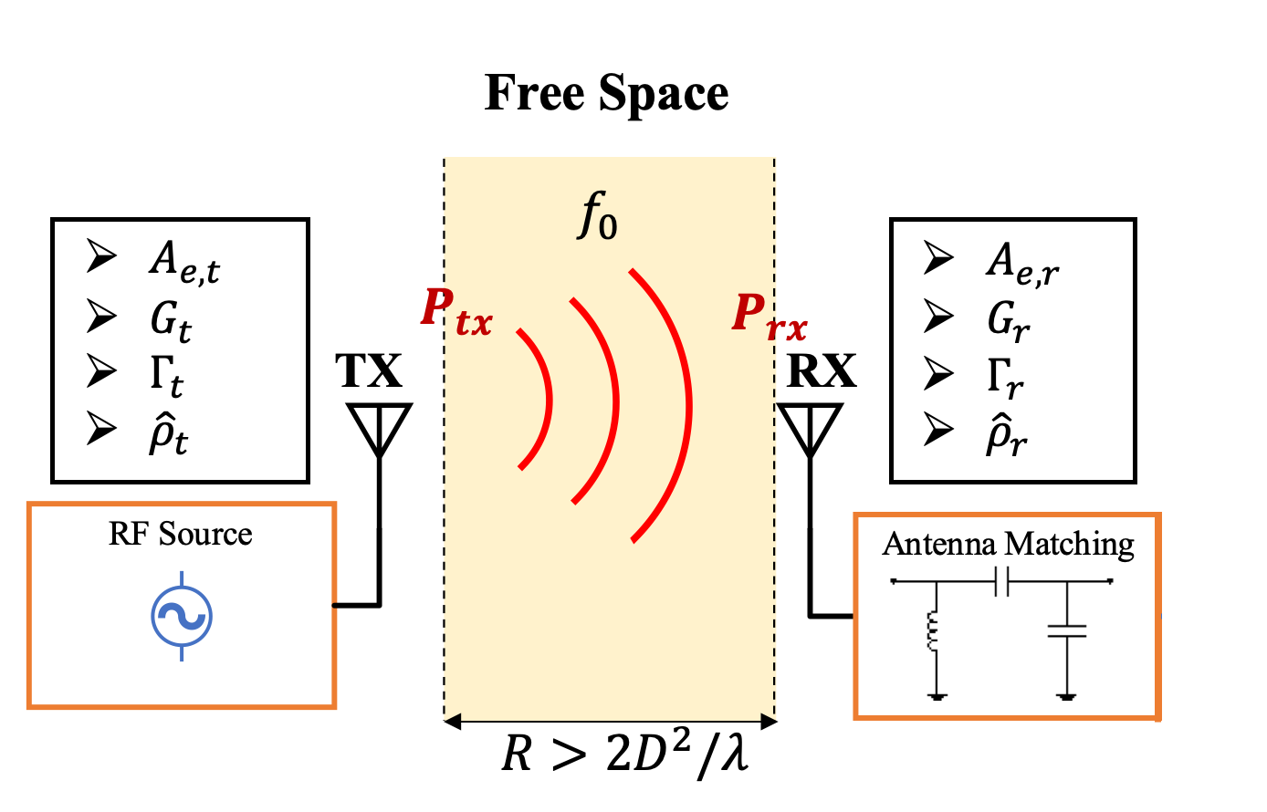 Figure 22 - Transmit and receive block diagram and associated variables that affect over-the-air RFEH system performance.
| Device | Effective Aperture (\(A_{\mathrm{e}}\)) | Gain | Reflection Coefficient (\(\Gamma\)) | Polarization (\(\hat{\rho}\)) | Max Linear Dimension (\(D\)) |
|---|---|---|---|---|---|
| TX | 513.6 cm\(^2\) | 15 dBi | \(<-15\) dB | Linear: vertical | 20.6 cm |
| RX | 38.1 cm\(^2\) | 3.7 dBi | \(<-15\) dB | Linear: horizontal | 2.5 cm |
The table above lists important parameters used for calculating the transmitter-to-receiver link budget based on the Friis equation given in (1). The received power versus distance from the transmitter for a source power $P_\mathrm{t}=13$ dBm and frequency $f_0=2.1$ GHz is plotted in Fig. 23.
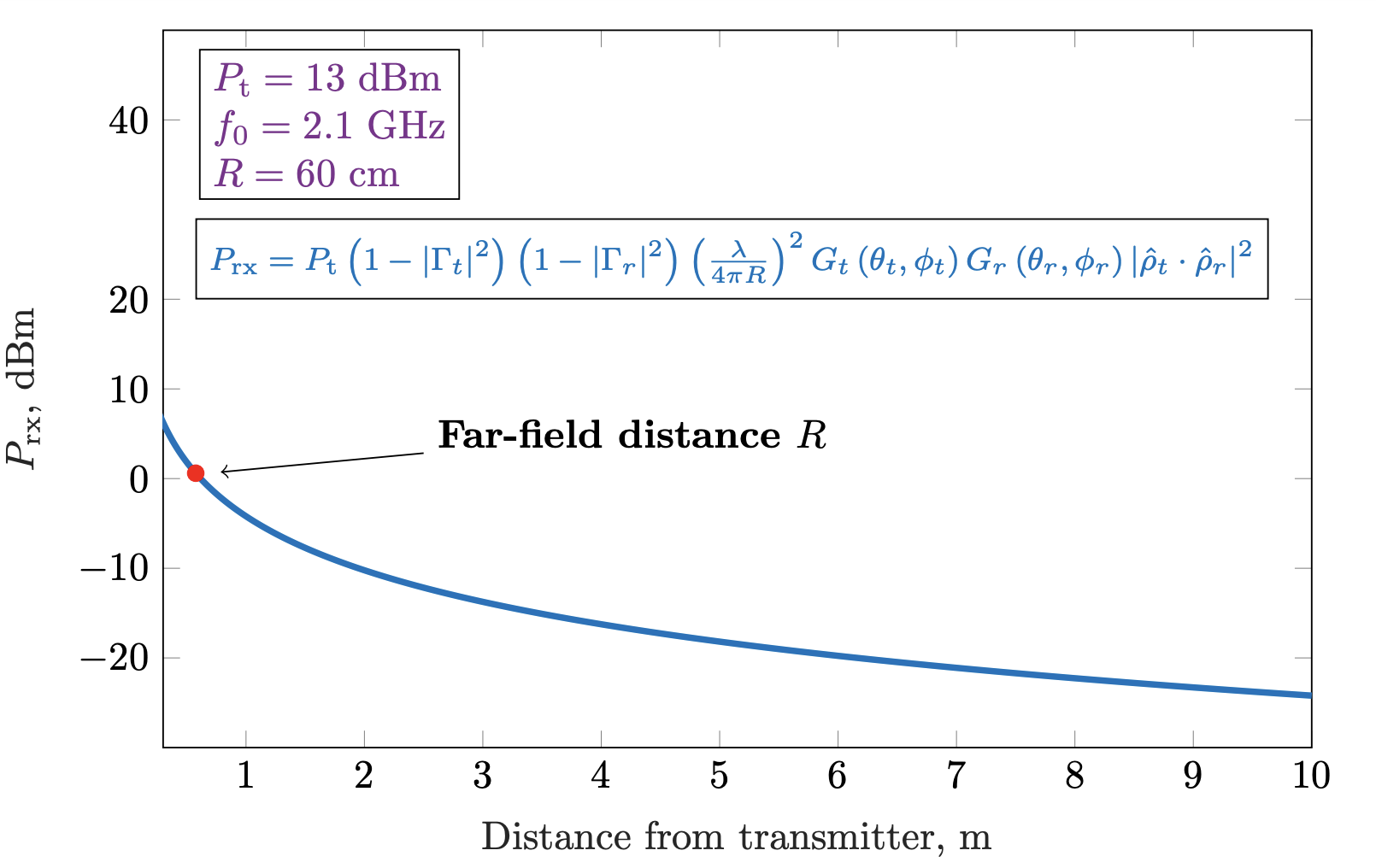 Figure 23 - Received power as a function of distance from the transmitter. The received power is calculated based on the Friis equation boxed in blue for a fixed test setup using the parameters in purple along with values from the table above
With an understanding of the received power levels able to be captured in the test setup, measurements are taken in order to characterize the system performance. The OTA measurement setup is shown in Fig. 24. The setup consists of an RF signal generator, a power amplifier, a power supply for DC biasing, a high-gain transmit antenna, the rectenna, a potentiometer, and a digital multi-meter. The power amplifier is used to slightly exceed the maximum output power of the RF signal generator. Note that in this test setup, the peak EIRP of the transmitter is 27 dBm.
The resulting output voltage versus load resistance for different incident power densities \(S_\mathrm{i}\) is shown in Fig. 25. This curve follows the same trend shown in the conducted mode output voltage measurements (see Fig. 20). The green curve represents the output voltage for the maximum incident power density able to be achieved for a transmitter-to-receiver separation distance equal to the far-field distance of about \(62\) cm.
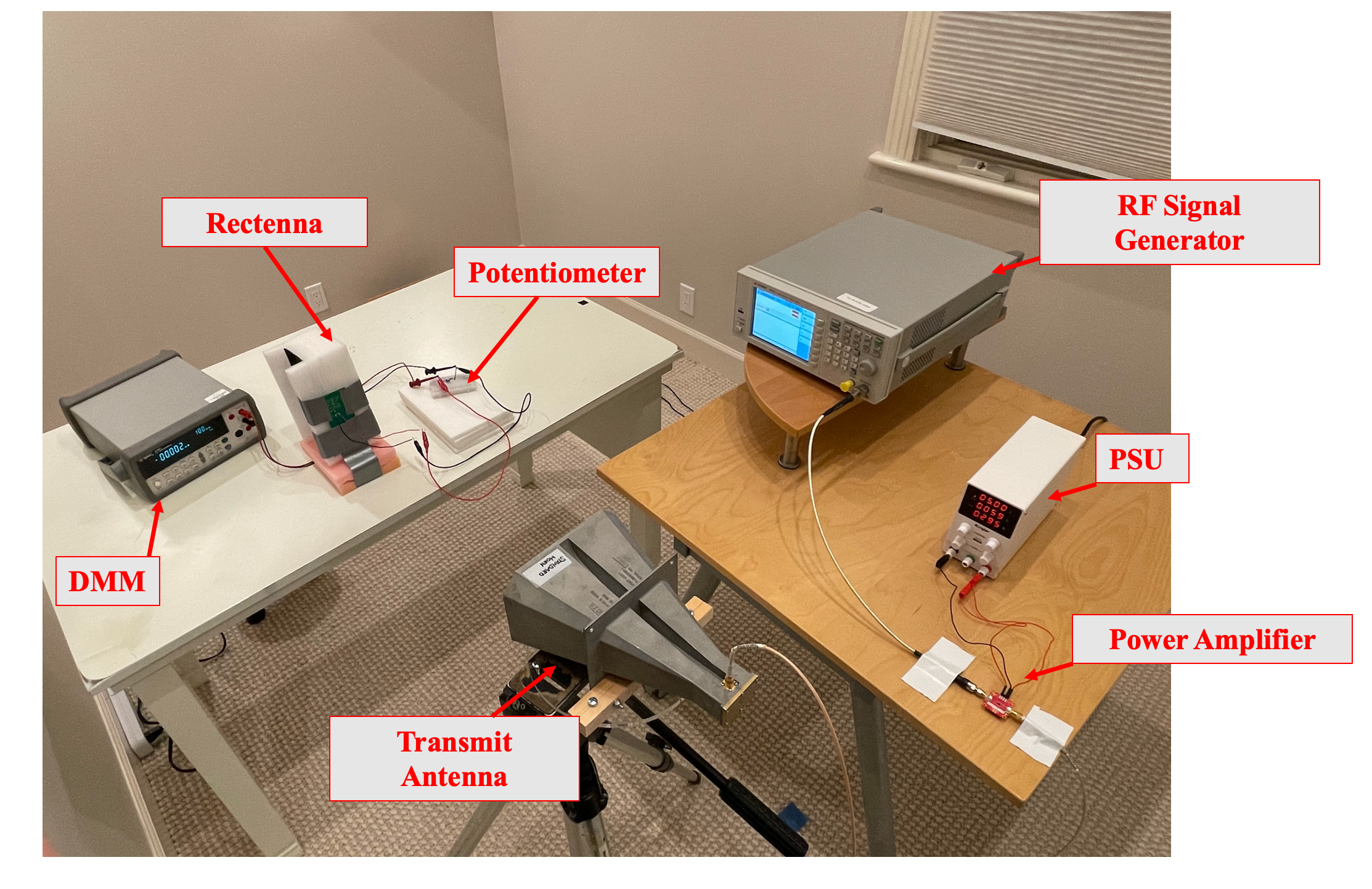 Figure 24 - OTA system characterization test setup.
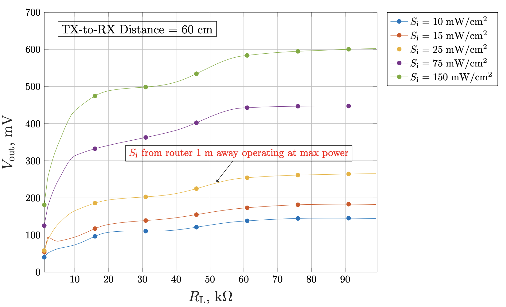 Figure 25 - Output voltage \(V_{\mathrm{out}}\) vs. load resistance \(R_\mathrm{L}\) for different incident power densities \(S_{i}\). The orange curve corresponds to an approximate incident power density one would observe standing 1 m away from a router transmitting at a max EIRP of 36 dBm.
An Application
To prove the feasability of the RFEH system, a simple test is carried out to power an off-the-shelf digital temperature sensor using the optimized rectenna design.
Operation & Block Diagram
Figure 26 abstracts the sensor load in block diagram format. The sensor load consists of a commercially-available PMU, rechargeable battery, microcontroller (MCU), and sensor.
The PMU selected was the TIBQ25570, which functions as a boost charger for the battery and hosts a maximum power point tracking feature (MPPT) 24. The MPPT tries to optimize the power extraction process, and in doing so, indirectly modulates the input impedance. From the PMU, the battery can be charged and is then used to power the MCU and sensor. The MCU collects data from the sensor, and sends it to the computer via a serial port. The MCU (MSP430FR5969 Launchpad Development Kit) was designed for low power operation, with multiple communication protocols including I2C, UART, and SPI 25. The temperature sensor, TMP116, is a digital, low-powered sensor with SMBUS- and I2C-compatible interfaces 26. See the table below for sensor load application specifications.
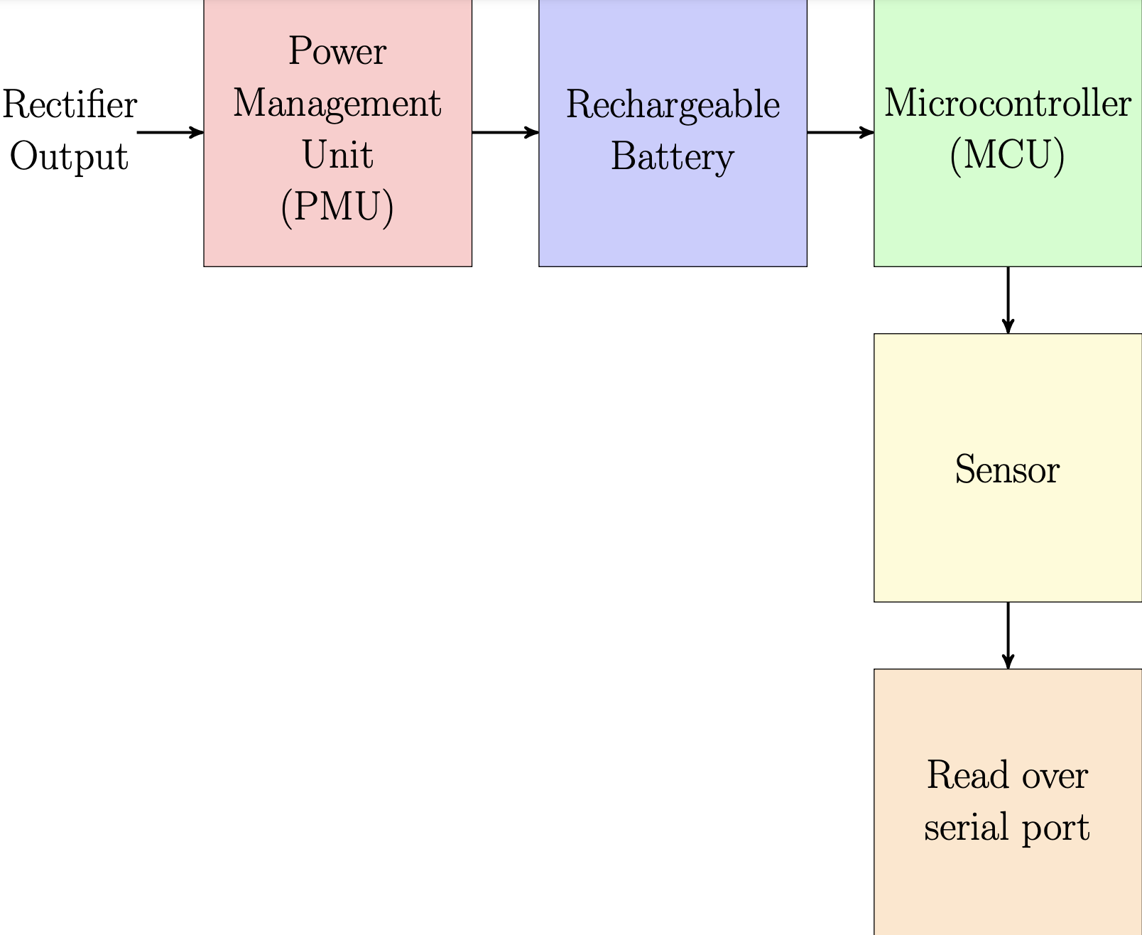 Figure 26 - Block diagram of sensor load.
| PMU | MCU | Sensor | |
|---|---|---|---|
| Min. Cold Start (V) | 0.6 | - | - |
| Min. Operation (V) | 0.1 | 1.8 | 1.9 |
OTA Integrated Rectenna and Sensor Load Testing
For final validation, the entire integrated system was examined. The test setup, shown in Fig. 27, is similar to the previous section describing the OTA rectenna setup, with a horn antenna as the transmitter and the rectenna as the receiver connected to the sensor load.
The test was conducted over 8 hours with the transmitter remotely powering the sensor, with success deemed when data was logged. Fig. 18 shows results comparing the rectenna and sensor load to only the sensor load, which was solely powered by battery. The battery-powered sensor load only lasted for 2 hours (red curve), while the rectenna charged the sensor load for the entire 8 hours (blue curve).
Based on this test, the rectenna system was able to successfully charge the sensor load for an extended period of time. However, the rectenna system was unable to overcome the PMU’s cold-start mode due to the fact that the rectifier was designed for a 10 k\(\Omega\) static load, which does not accurately reflect the PMU’s varying impedance as a result of its MPPT feature. Nevertheless, the test is still able to demonstrate that the rectenna system works in a steady state operational mode.
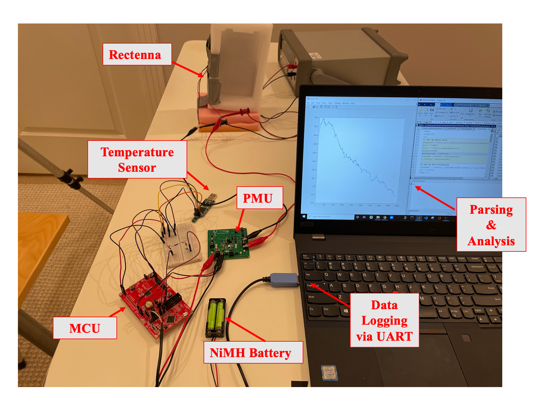 Figure 27 - Setup of rectenna and sensor load.
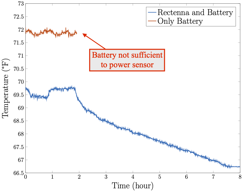 Figure 28 - OTA test with sensor load vs. only sensor load over 8 hours.
Design Challenges
In the course of system bring-up, tuning, and preliminary system-level tests, it was found to be difficult to synthesize a matching network with the rectifier at the original design frequency of \(f_0 = 2.45\) GHz. Matching a rectifier to the system impedance \(Z_0\) is difficult as the rectifier input impedance at \(f_0\) will vary depending on load conditions and input power. Effectively, when a matching network is synthesized for one particular impedance measurement, the input power to the rectifier increases. This leads to a change of input impedance of the rectifier due to the non-linear response of the diodes, and results in the rectifier not being matched again.
To help deal with this issue, the circuit model of the PCB, traces, and vendor lumped element models were prototyped in ADS in order to gain an understanding of how the circuit changes as a function of these parameter values, as well as the relative input power \(P_{\mathrm{in}}\) and DC load resistance \(R_\mathrm{L}\). Utilizing the Harmonic Balance simulator in conjunction with the optimization controller led to close agreement between the raw input impedance measurement to the rectifier for both the measured and simulated response as is seen in Fig. 29.
Despite the agreement between the raw input impedance measurements of the model and PCB, synthesizing a matching network based on ADS optimization was not initially able to be accomplished at \(f_0 = 2.45\) GHz. However, it was found that shifting to a slightly lower frequency of \(f_0 = 2.1\) GHz was able to produce a solid matching network that was reliably measured on multiple boards. In the interest of time, this matching network was implemented on all of the PCB variants in order to conduct system-level tests of the design. Additionally, the antenna was simply re-matched to this frequency using the extra $$\pi$-topology pads included on the PCB.
The initial antenna characterization was validated against the raw simulation model using the original design frequency of $f_0 = 2.45$ GHz. The simulated, measured, and matched \(S_{11}\) responses for this design frequency are shown in Fig. 29.
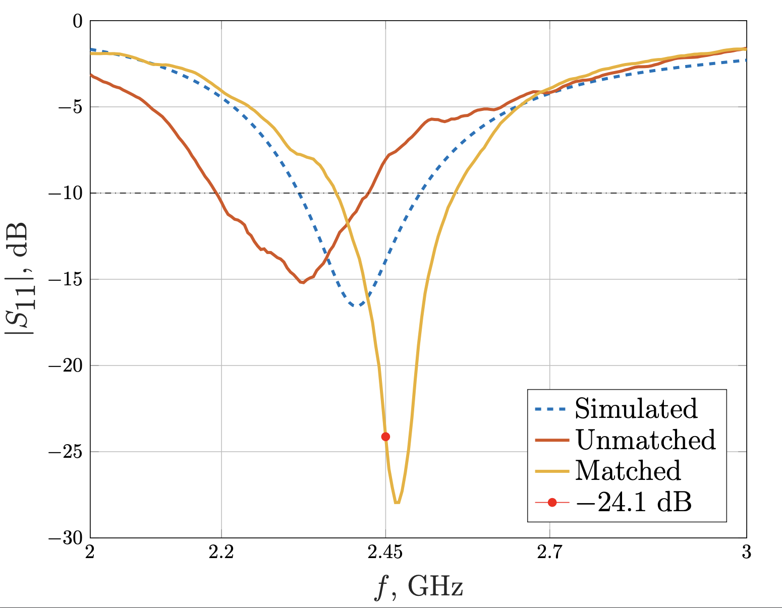 Figure 29 - Simulated, measured, and matched \(S_{11}\) of PIFA antenna at original design frequency \(f_0=2.45\) GHz.
After system-level tests using the new frequency of \(f_0=2.1\) GHz, it was observed that switching to a higher frequency rated component library was able to produce an acceptable rectifier matching level at \(2.45\) GHz. Lumped components have a self-resonant frequency (SRF), which helps to characterize their parasitic behavior. In essence, an inductor acts like an inductor up to its SRF, and likewise for a capacitor. When the component operates in a region above its SRF, then its parasitic behavior will affect performance.
The synthesized matching network along with the \(S_{11}\) response is shown in Fig. 30. Once again, in the interest of time, this network was not implemented for system-level testing. However, further work on this project should use this matching circuit as the operation at $2.45$ GHz is in the FCC unlicensed ISM band 27.
| Smith Chart | Log Magnitude |
|---|---|
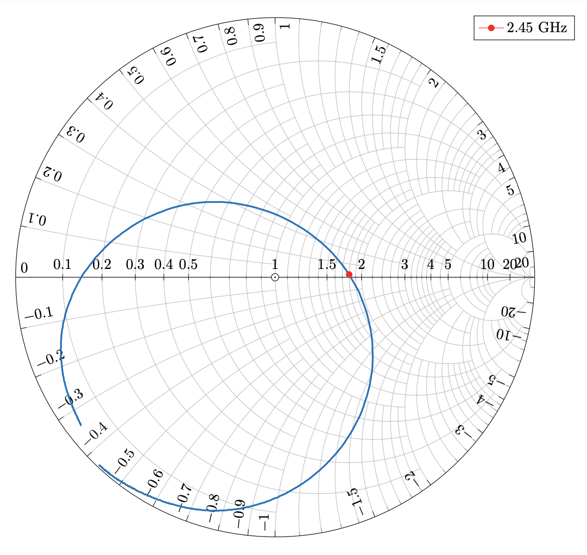 |
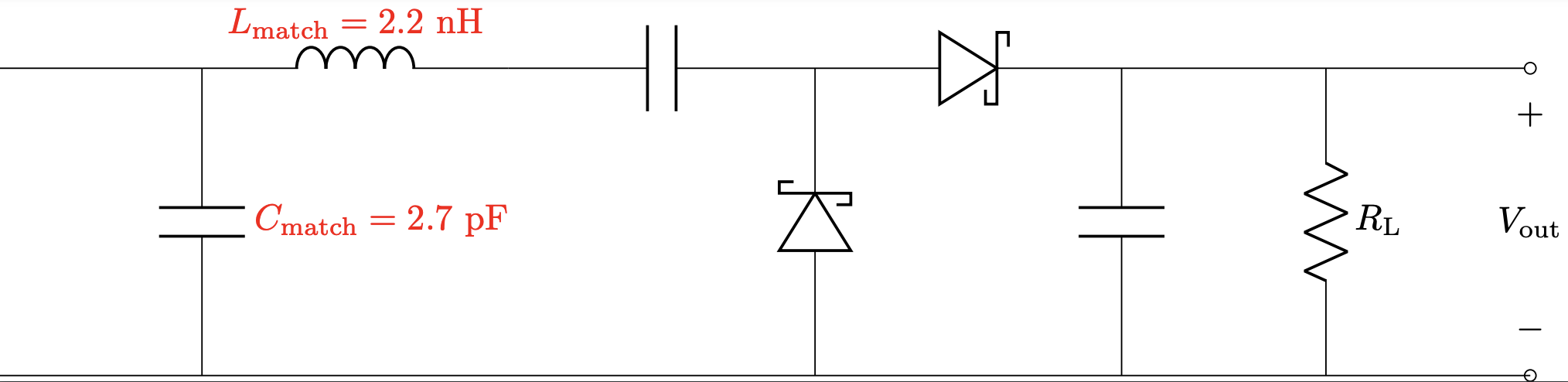 Figure 30 - $f_0=2.45$ GHz rectifier matching network (bottom), Smith Chart (top left), and log-magnitude response (top right).
Conclusions
The goal of this project was to display the validity of RFEH by designing and validating our own custom solution capable of powering an IoT sensor. This work was motivated by an increasing reliance on IoT devices, and thus, a demand for more power to be delivered in an efficient and sustainable fashion. In doing so, robust simulations were conducted using powerful solvers and modern techniques such as ADS and HFSS. The design was then laid out and fabricated. Extensive tests in different conditions validated our system and provided proof of the system’s ability to power a commercial IoT temperature sensor. Assessing our performance, original objectives were achieved and when faced with technical challenges, the project was appropriately adapted in a manner that successfully validated our system.
We have outlined a few tasks to further improve our design:
- Performing electromagnetic co-simulation of the PCB with lumped components and diode models, thereby providing a comprehensive simulation that accounts for component and trace parasitics
- Integrating the PMU and sensor load onto the remaining PCB area to create a compact and comprehensive system
- Analyzing the fabricated antenna in an anechoic chamber for OTA characterization
- Exploring input signal optimization to improve RF-to-DC conversion efficiency.
Overall, this project has demonstrated many of the exciting and emerging applications of RFEH, and has served to open innovation for future researchers.
References
N. Tesla, “The transmission of electrical energy without wires as a means for furthering peace,” Electrical World and Engineer, p. 21–24, 1905. ↩
J. Koomey, S. Berard, M. Sanchez, and H. Wong, “Implications of historical trends in the electrical efficiency of computing,” IEEE Annals of the History of Computing, vol. 33, no. 3, pp. 46–54, 2011. ↩ ↩2
S. Nikoletseas, Y. Yang, and A. Georgiadis, Wireless Power Transfer Algorithms, Technologies and Applications in Ad Hoc Communication Networks. Gewerbestrasse 11, 6330 Cham, Switzerland: Springer International Publishing AG, 2016. ↩ ↩2 ↩3
T. Jury, “How many iot devices are there in 2020? [Online]. Available: https://techjury.net/blog/how-many-iot-devices-are-there. ↩
W. C. Brown, “Microwave to dc converter,” U.S. Patent 3434678A, May. 1969. ↩
S. Keyrouz, “Practical rectennas, rf power harvesting and transport,” Ph.D. dissertation, Eindhoven University of Technology, Eindhoven, The Netherlands, 2014. ↩
. Paing, J. Morroni, A. Dolgov, J. Shin, J. Brannan, R. Zane, and Z. Popovic, “Wirelessly-powered wireless sensor platform,” in 2007 European Conference on Wireless Technologies, 2007, pp. 241–244. ↩
S. M. Asif, A. Iftikhar, J. W. Hansen, M. S. Khan, D. L. Ewert, and B. D. Braaten, “A novel rf-powered wireless pacing via a rectenna-based pacemaker and a wearable transmit-antenna array,” IEEE Access, vol. 7, pp. 1139–1148, 2019. ↩
J. T. Bernhard, K. Hietpas, E. George, D. Kuchima, and H. Reis, “An interdisciplinary effort to develop a wireless embedded sensor system to monitor and assess corrosion in the tendons of prestressed concrete girders,” in 2003 IEEE Topical Conference on Wireless Communication Technology, 2003, pp. 241–243. ↩
A. Zhao, H. Gao, G. Zhang, B. Ayhan, F. Yan, C. Kwan, and J. L. Rose, “Active health monitoring of an aircraft wing with embedded piezoelectric sensor/actuator network: I. defect detection,localization and growth monitoring,” Smart Materials and Structures, vol. 16, no. 4, pp. 1208–1217, jun 2007. [Online]. Available: https://doi.org/10.1088\%2F0964-1726\%2F16\%2F4\%2F032. ↩
C. A. Balanis, Antenna theory: analysis and design. Wiley-Interscience, 2005. ↩ ↩2 ↩3 ↩4
M. Nie, X. Yang, G. Tan, and B. Han, “A compact 2.45-ghz broadband rectenna using grounded coplanar waveguide,” IEEE Antennas and Wireless Propagation Letters, vol. 14, pp. 986–989, 2015. ↩
H. J. Visser and R. J. M. Vullers, “Wireless sensors remotely powered by rf energy,” in 2012 6th European Conference on Antennas and Propagation (EUCAP), 2012, pp. 1–4. ↩ ↩2 ↩3
Y. Taryana, Y. Sulaeman, A. Setiawan, T. Praludi, and E. Hijriani, “Rectifying antenna design for wireless power transfer in the frequency of 2.45 ghz,” in 2018 International Conference on Radar, Antenna, Microwave, Electronics, and Telecommunications (ICRAMET), 2018, pp. 55–58. ↩
G. Andia Vera, A. Georgiadis, A. Collado, and S. Via, “Design of a 2.45 ghz rectenna for electromagnetic (em) energy scavenging,” in 2010 IEEE Radio and Wireless Symposium (RWS), 2010, pp.61–64. ↩ ↩2
A. Hirono, N. Sakai, and K. Itoh, “High efficient 2.4ghz band high power rectenna with the direct matching topology,” in 2019 IEEE Asia-Pacific Microwave Conference (APMC), 2019, pp. 1268–1270. ↩
. Lin, C. Chiu, and J. Gong, “A wearable rectenna to harvest low-power rf energy for wireless health-care applications,” in 2018 11th International Congress on Image and Signal Processing, BioMedical Engineering and Informatics (CISP-BMEI), 2018, pp. 1–5. ↩
S. A. Maas, Nonlinear microwave and RF circuits; 2nd ed. Boston: Artech House, 2003. [Online]. Available: https://bib-pubdb1.desy.de/record/387459. ↩
H. J. Visser, Approximate Antenna Analysis for CAD. Chichester, U.K: Wiley, 2009. ↩ ↩2
M. M. Mansour and H. Kanaya, “Compact and broadband rf rectifier with 1.5 octave bandwidth based on a simple pair of l-section matching network,” IEEE Microwave and Wireless Components Letters, vol. 28, no. 4, pp. 335–337, 2018. ↩
LQW03AW3N6C00, Skyworks Solutions. [Online]. Available: https://www.murata.com/en-us/productsproductdetail?partno=LQW03AW3N6C00%23]. ↩
SMS7630 SERIES, Skyworks Solutions, 2021. [Online]. Available: https://www.skyworksinc.com/-/media/SkyWorks/Documents/Products/201-300/Surface Mount Schottky Diodes 200041AG.pdf. ↩
RT/duroid® 6006/6010LM, Rogers Corporation. [Online]. Available: https://rogerscorp.com/-/media/project/rogerscorp/documents advanced-connectivity-solutions/english/data-sheets/rt-duroid-6006-6010lm-laminate-data-sheet.pdf ↩
Ultra Low Power Harvester Power Management IC with Boost Charger, Texas Instruments, 2019. [Online]. Available: https://www.ti.com/store/ti/en/p/product/?p=BQ25570RGRR. ↩
MSP430FR596x, MSP430FR594x Mixed-Signal Microcontrollers, Texas Instruments, 2019. [Online]. Available: https://www.ti.com/lit/ds/symlink/msp430fr5969.pdf?ts=1622520995734. ↩
TMP116 High-Accuracy, Low-Power, Digital Temperature Sensor With SMBus- and I2C-Compatible Interface, Texas Instruments, May 2017. [Online]. Available: https://www.ti.com/lit/ds/symlink/tmp116.pdf?ts=1622565910533. ↩
Equipment authorization – rf device.” [Online]. Available: https://www.fcc.gov/oet/ea/rfdevice. ↩